Radio frequency LDMOS device with buried layer below drain electrode

A drain and radio frequency technology, applied in the direction of semiconductor devices, electrical components, circuits, etc., can solve the problems of reducing device breakdown voltage, LDMOS early breakdown, device failure, etc., and achieve the effect of increasing breakdown voltage

Inactive Publication Date: 2012-11-21
HUAZHONG UNIV OF SCI & TECH
View PDF6 Cites 8 Cited by
  • Summary
  • Abstract
  • Description
  • Claims
  • Application Information

AI Technical Summary

Problems solved by technology

This will not only cause the LDMOS to break down early and reduce the breakdown voltage of the device; but also due to the hot carrier effect, the hot carrier will bombard the gate oxide layer and even cause the device to fail

Method used


Image

  • Radio frequency LDMOS device with buried layer below drain electrode
  • Radio frequency LDMOS device with buried layer below drain electrode

Examples


Embodiment Construction

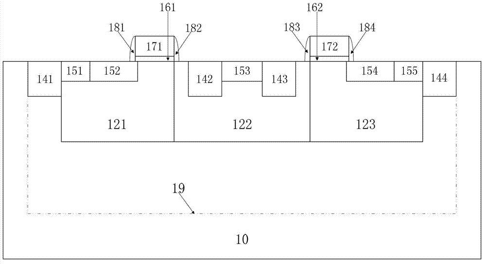
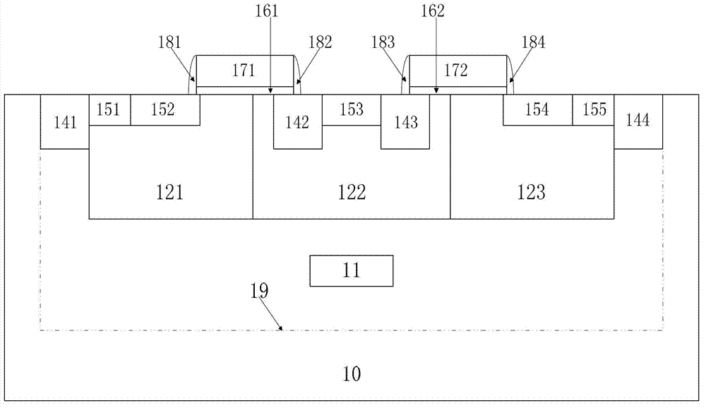
[0029]see figure 1 with figure 2 The difference between the LDMOS device of the present invention and the traditional LDMOS device is that: the gate 171 and the gate 172 are moved to the top of the STI142 and the STI143 near the drain terminal respectively; Inner (p-type LDMOS) introduces a buried layer 11 whose doping type is opposite to that of the source and drain.

[0030] Gate 171 and gate 172 are moved to the top of STI142 and STI143 near the drain terminal respectively, that is, gate plate 171 overlaps with STI142, and gate plate 172 overlaps with STI143; change from 0 to the lateral width of STI142 or STI143. The specific value of the above overlapping length needs to be optimized according to the process parameters and the specific structural parameters of the device. The higher the concentration of the well 122 serving as the drift region and the deeper the well, the greater the overlapping length.

[0031] The parameters of the introduced buried layer 11 include ...


PUM


Abstract

The invention discloses a radio frequency LDMOS (Laterally Diffused Metal Oxide Semiconductor) device with a buried layer below a drain electrode which is improved at two aspects aiming at traditional radio frequency LDMOS breakdown voltage, that is grid electrode plates (171) and (172) are stretched and overlapped with an STI (142) and an STI (143); and the buried layer is rightly led below the drain electrode (153). The grid electrode plates are stretched onto the STIs, thus limitation of electric field peak on the breakdown voltage, wherein the electric field peak is led by the grid electrode plates; owing to the leading of the buried layer (11), the radio frequency LDMOS device is provided with n+n-p-p+ structure in the longitudinal direction, which facilitates exhaustion of a drift region rightly below the drain electrode (153), so that the longitudinal electric field is equalized, and breakdown voltage of the radio frequency LDMOS device is improved. In addition, the buried layer (11) is located outside the drift region, is far from a current-carrying subchannel, so that the frequency characteristic of the radio frequency LDMOS device is hardly affected. Therefore, the structure of the radio frequency LDMOS device is particularly suitable for a radio frequency power device, can effectively improve performance of a radio frequency power amplifier (PA).

Description

technical field [0001] The invention belongs to the technology of high-voltage power integrated circuits, and in particular relates to a radio frequency LDMOS (laterally diffused MOS transistor) device with a buried layer under the drain. Background technique [0002] see figure 1 , which is an existing LDMOS device with the well as the body and the drift region (that is, for n-type LDMOS, the p well is used as the body region, and the n well is used as the drift region; for the p-type LDMOS, the n well is used as the body region, p-well as the drift region.) Schematic cross-section. The figure shows an LDMOS device structure with two interdigitated fingers, that is, the two LDMOS devices share a drain 153; 19 is a deep n well, which is only used for p-type LDMOS. [0003] For n-type LDMOS, 121 and 123 are p-wells, and 122 is an n-well. The n-well and the p-well are located at a deeper position from the surface of the device to the substrate 10, and the p-well and the n-w...

Claims


Application Information

Patent Timeline
Patent Type & Authority Applications(China)
IPC IPC(8): H01L29/78H01L29/06
Inventor 陈晓飞沈亚丁邹望辉邹雪城
Owner HUAZHONG UNIV OF SCI & TECH
Why Eureka
Try Eureka