A semi-superjunction lateral double-diffused metal-oxide-semiconductor field-effect transistor with a stepped n-type heavily doped buried layer

An oxide semiconductor and lateral double-diffusion technology, which is applied in semiconductor devices, electrical components, circuits, etc., can solve the problems of breaking the charge balance, the P-type column region cannot be completely depleted, and reducing the lateral breakdown voltage of SJ-LDMOS devices. , to achieve the effect of increasing withstand voltage, low specific on-resistance, and improving longitudinal breakdown voltage

Active Publication Date: 2021-01-01
XIDIAN UNIV
View PDF5 Cites 0 Cited by
  • Summary
  • Abstract
  • Description
  • Claims
  • Application Information

AI Technical Summary

Problems solved by technology

[0004] However, for SJ-LDMOS, due to the substrate-assisted depletion of the N-type pillar region (or P-type pillar region), the P-type pillar region (or N-type pillar region) cannot be completely depleted when the device breaks down, breaking the N-type pillar region. The charge balance between the column area and the P-type column area reduces the lateral breakdown voltage of the SJ-LDMOS device

Method used


Image

  • A semi-superjunction lateral double-diffused metal-oxide-semiconductor field-effect transistor with a stepped n-type heavily doped buried layer
  • A semi-superjunction lateral double-diffused metal-oxide-semiconductor field-effect transistor with a stepped n-type heavily doped buried layer

Examples


Embodiment Construction

[0035] The present invention will be described below by taking N-channel LDMOS as an example in conjunction with the accompanying drawings.

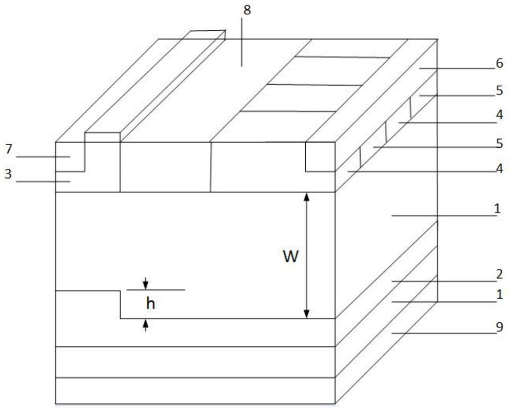
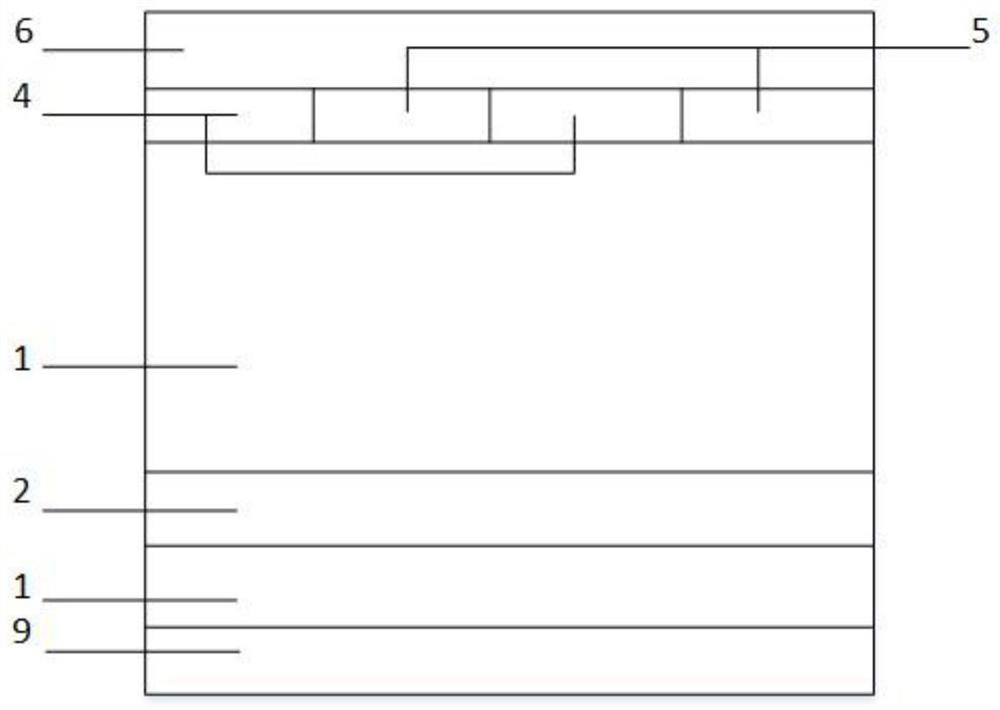
[0036] Such as figure 1 and figure 2 As shown, the present invention has a semi-superjunction lateral double-diffused metal oxide semiconductor field effect transistor with a stepped N-type heavily doped buried layer, including:

[0037] P-type substrate 9;

[0038] The P-type epitaxial layer 1 on the substrate is used as a buffer layer of the device;

[0039] A stepped N-type heavily doped buried layer 2 located inside the P-type epitaxial layer;

[0040] P-type base region 3 located on the surface of the P-type epitaxial layer;

[0041] N+ type source region 7 located on part of the surface of the P type base region;

[0042] N+ type drain region 6 located on part of the surface of the semi-superjunction region;

[0043] In the semi-superjunction area, the N-column 4 and the P-column 5 are arranged at intervals in the lateral cy...


PUM


Abstract

The invention provides a semi-super-junction lateral double-diffused metal oxide semiconductor field-effect transistor with a stepped N-type heavily-doped buried layer. An N-type drift assisted regionis formed in a middle region of the upper portion of a P-type epitaxial layer; the left end of the N-type drift assisted region is adjacent to a P-type base region, and the right end of the N-type drift assisted region is adjacent to a semi-super-junction region; the stepped N-type heavily-doped buried layer is arranged in the P-type epitaxial layer; the distance W between the upper end of the relatively thin N-type heavily-doped buried layer and the semi-super-junction region meets the requirement that the P-type epitaxial layer above the relatively thin N-type heavily-doped buried layer iscompletely depleted; and the step height h of the stepped N-type heavily-doped buried layer is matched with the heavy doping concentration. While a substrate-assisted depletion effect is realized, electric field distribution of a drain end and a source end is adjusted to further optimize a contradiction relation between a breakdown voltage and specific on-resistance, thereby realizing high breakdown voltage and low specific on-resistance.

Description

technical field [0001] The invention relates to the technical field of semiconductor power devices, in particular to a semi-superjunction lateral double-diffused metal oxide semiconductor field effect transistor. Background technique [0002] The lateral power semiconductor device LDMOS (Lateral Double-diffused MOSFET) is the key technology of the high-voltage integrated circuit HVIC (High Voltage Integrated Circuit) and the power integrated circuit PIC (Power Integrated Circuit). Its main feature is that a relatively long lightly doped drift region is added between the base region and the drain region, and the doping type of the drift region is consistent with that of the drain region. By adding the drift region, it can share the breakdown voltage, improve the breakdown voltage of the LDMOS, make it achieve the optimization goal of low on-resistance, and minimize the conduction loss. Because of its high breakdown voltage, low on-resistance, and easy integration with low-vo...

Claims


Application Information

Patent Timeline
Patent Type & Authority Patents(China)
IPC IPC(8): H01L29/06H01L29/78
CPCH01L29/0634H01L29/0692H01L29/7816
Inventor 黄俊杰段宝兴杨鑫杨银堂
Owner XIDIAN UNIV
Why Eureka
Try Eureka