High-k dielectric trench lateral superjunction double-diffused metal oxide wide bandgap semiconductor field effect transistor and manufacturing method thereof
A field effect transistor and semiconductor technology, applied in the field of lateral superjunction double diffusion metal oxide semiconductor field effect transistors
- Summary
- Abstract
- Description
- Claims
- Application Information
AI Technical Summary
Problems solved by technology
Method used
Image
Examples
Embodiment Construction
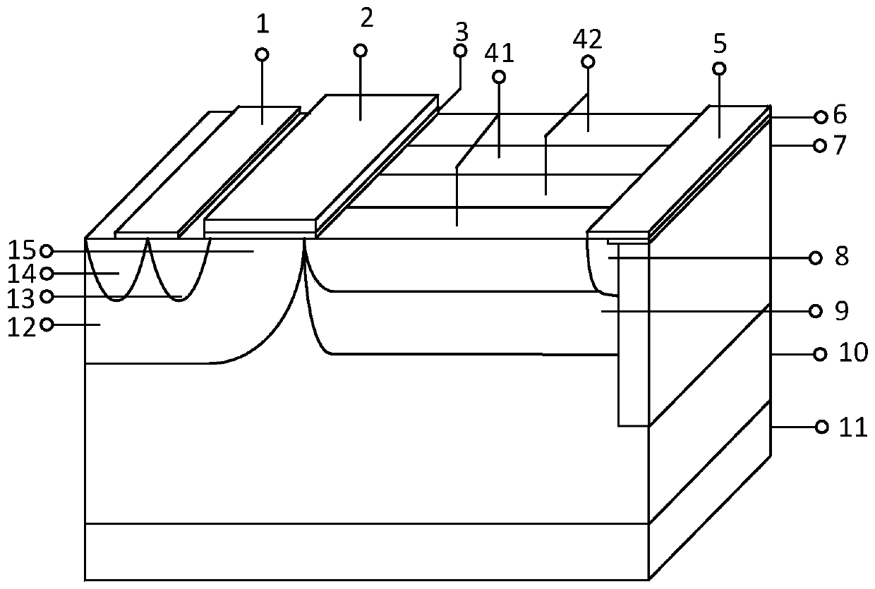
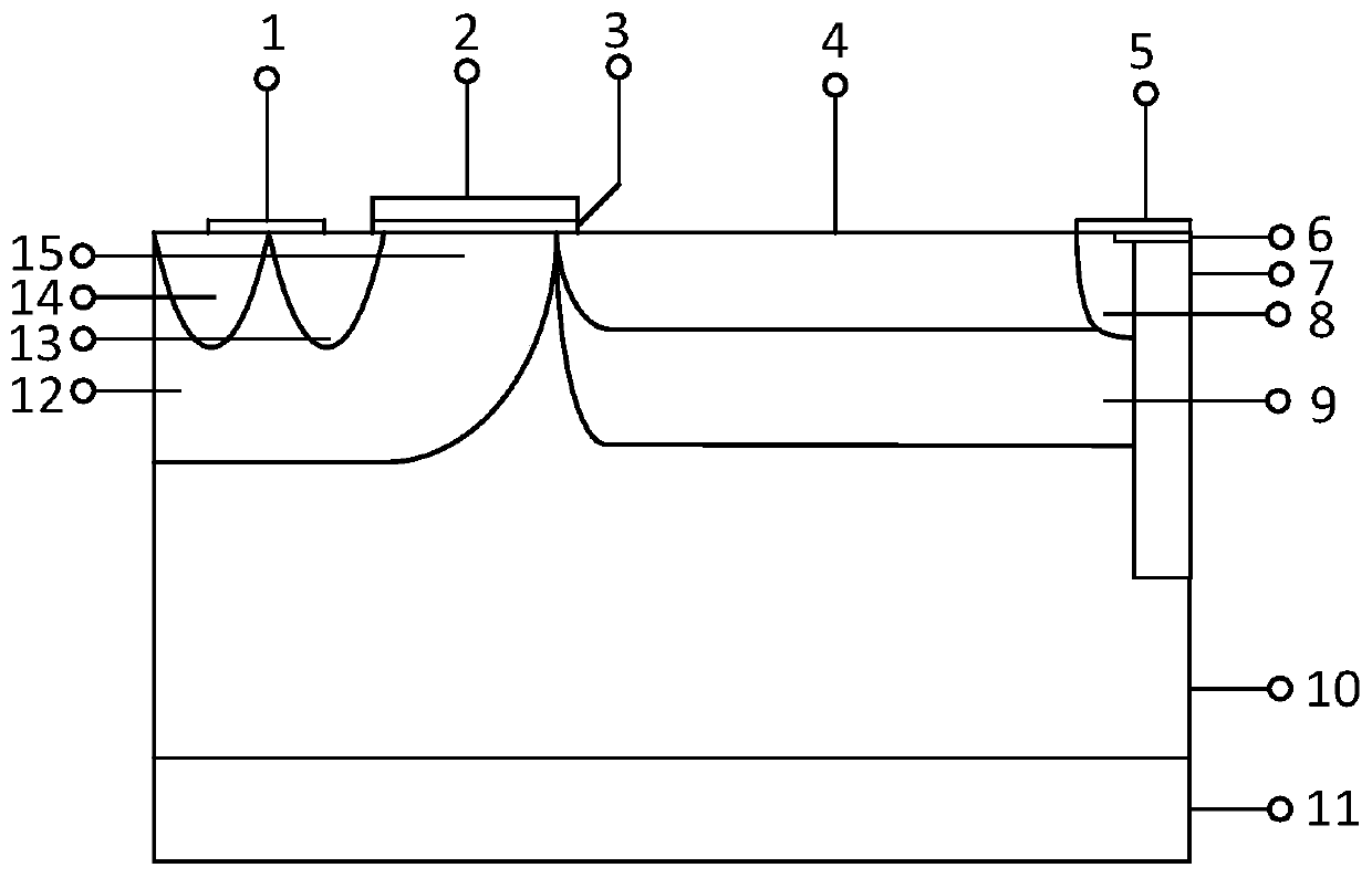
[0049] Such as figure 1 , figure 2 As shown, the lateral superjunction double-diffused metal oxide wide bandgap semiconductor field effect transistor of the high-K dielectric trench proposed by the present invention includes:
[0050] A substrate 11 of a wide bandgap semiconductor material (such as gallium nitride, silicon carbide or diamond) (the doping concentration of the substrate is 1×10 13 cm -3 ~1×10 15 cm -3 );
[0051] an epitaxial layer 10 grown on a substrate;
[0052] The base region 12 and the buffer layer 9 formed on the epitaxial layer; the product of the doping concentration of the buffer layer and the thickness of the buffer layer satisfies the principle of charge balance to eliminate the substrate-assisted depletion effect; the doping concentration of the buffer layer is 1×10 14 cm -3 ~1×10 16 cm -3 ;
[0053]The super junction drift region 4 formed on the buffer layer is composed of several N columns 41 and P columns 42 arranged alternately; the d...
PUM
| Property | Measurement | Unit |
|---|---|---|
| relative permittivity | aaaaa | aaaaa |
Abstract
Description
Claims
Application Information

