Array substrate and manufacturing method thereof and display device

A technology of an array substrate and a manufacturing method, which is applied in the display field and can solve the problems of small viewing angle and single deflection angle, etc.

Active Publication Date: 2015-12-09
BOE TECH GRP CO LTD
View PDF7 Cites 6 Cited by
  • Summary
  • Abstract
  • Description
  • Claims
  • Application Information

AI Technical Summary

Problems solved by technology

[0004] However, in the existing array substrates, the structure of each pixel unit is usually basically the same, and the liquid crystal molecules in the corresponding liquid crystal region have a single deflecti...

Method used


Image

  • Array substrate and manufacturing method thereof and display device
  • Array substrate and manufacturing method thereof and display device
  • Array substrate and manufacturing method thereof and display device

Examples


Embodiment 1

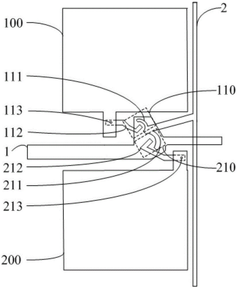
[0098] Such as figure 1 As shown, the pixel unit specifically includes a first sub-pixel electrode 100 and a second sub-pixel electrode 200, and a first charging thin film transistor 110 and a second charging thin film transistor 210. The first charging thin film transistor 110 includes a charging source 111, a charging drain electrode 112 and charging grid (the charging grid corresponds to the channel between the charging source 111 and the charging drain 112 in the figure, and is located at the lower layer of the source-drain metal layer where the source 111 and the drain 112 are located and the gate line 1 electrical connection, not shown in the figure), the second charging thin film transistor 210 includes a charging source 211, a charging drain 212 and a charging gate (the charging gate is electrically connected to the gate line 1, and the charging The gate is located below the channel between the charging source 211 and the charging drain 212 in the figure, and is locate...

Embodiment 2

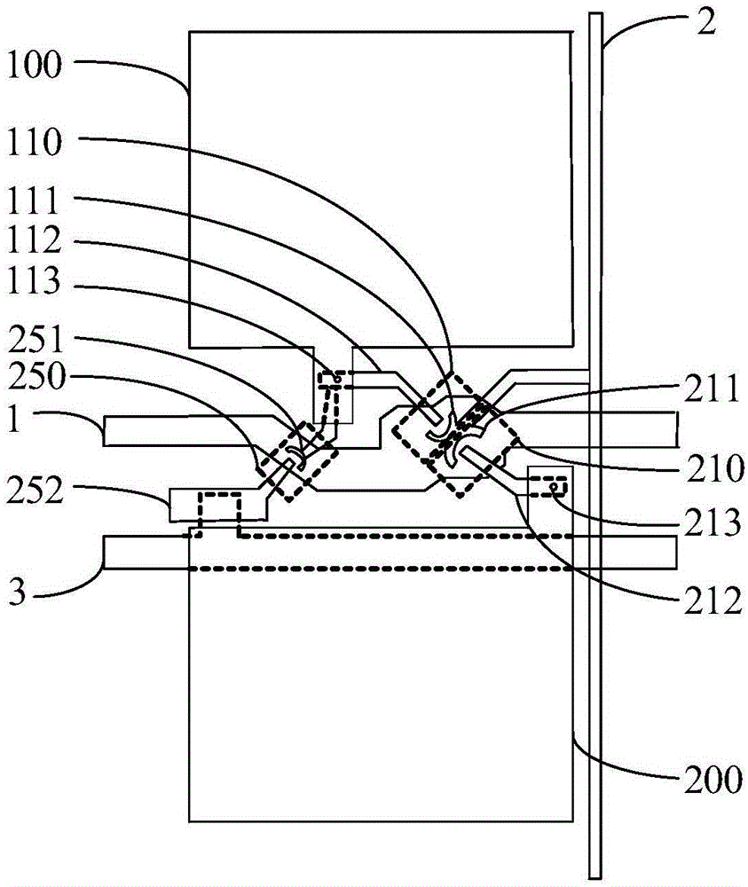
[0104] Such as figure 2 As shown, in this embodiment, in the same pixel unit, a voltage-dividing thin film transistor 250 is also included. The voltage-dividing thin film transistor 250 includes a voltage-dividing source 251, a voltage-dividing drain 252, and a gate. The voltage-dividing source 251 and The first sub-pixel electrode 100 is electrically connected, a voltage-dividing drain 252 is formed corresponding to the voltage-dividing source 251, a channel is formed between the voltage-dividing source 251 and the voltage-dividing drain 252, and the voltage-dividing drain 252 extends to the common electrode line 3 Directly above , together with the common electrode line 3 constitute a step-down storage capacitor. In the embodiment of the present invention, a specific setting method of the voltage-dividing thin film transistor 250 and the step-down storage capacitor is provided, but it is not limited thereto. Those skilled in the art can set the voltage-dividing thin film tr...

Embodiment 3

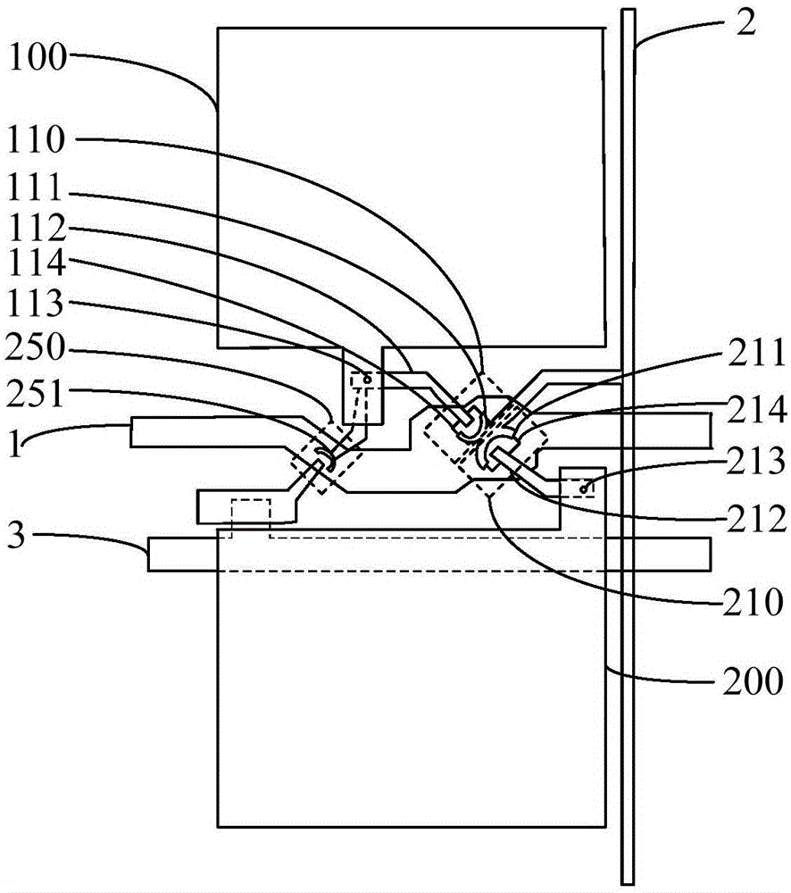
[0106] Such as image 3 As shown, as mentioned above, the charging current of the thin film transistor is proportional to the aspect ratio and / or the carrier mobility of the active layer. Therefore, in this embodiment, by making the first charging thin film transistor The carrier mobility of the material of the active layer 114 in 110 is smaller than the carrier mobility of the material of the active layer 214 in the second charging thin film transistor 210, so as to further make the charging capability of the second charging thin film transistor 110 higher than that of the first charging thin film transistor. The charging capability of the charging TFT 210 is stronger, so that the charging voltage of the first sub-pixel electrode 100 is lower than the charging voltage of the second sub-pixel electrode 200 . Furthermore, the deflection angles of the liquid crystal molecules in the liquid crystal regions corresponding to the same pixel unit are different, and finally the viewin...


PUM


Abstract

The embodiment of the invention provides an array substrate and a manufacturing method thereof and a display device and relates to the technical field of display. The visual angle characteristic of the liquid crystal display device is improved. The array substrate comprises multiple pixel units. At least one pixel unit comprises a first sub-pixel electrode and a second sub-pixel electrode. The first sub-pixel electrodes are electrically connected with first charging thin film transistors, and the second sub-pixel electrodes are electrically connected with second charging thin film transistors. In the same pixel unit, the charging capacity of the second charge thin film transistors is higher than that of the first charging thin film transistors. The manufacturing method is the manufacturing method of the array substrate provided in the technical scheme. The liquid crystal display device comprises the array substrate provided in the technical scheme. The array substrate and the manufacturing method thereof can be used for the liquid crystal display device.

Description

technical field [0001] The present invention relates to the field of display technology, in particular to an array substrate, a manufacturing method thereof, and a display device. Background technique [0002] Liquid crystal display devices have the characteristics of low power consumption and no radiation, and have now occupied a dominant position in the field of flat panel displays. [0003] A liquid crystal panel in an existing liquid crystal display device usually includes an array substrate and a color filter substrate disposed opposite to each other, and a liquid crystal layer filled between the array substrate and the color filter substrate. Each pixel unit is provided with a pixel electrode, corresponding to the pixel electrode, and a common electrode is provided on the color filter substrate, through the electric field formed between the pixel electrode and the common electrode, the liquid crystal molecules in the liquid crystal region corresponding to the pixel uni...

Claims


Application Information

Patent Timeline
IPC IPC(8): G02F1/1362G02F1/1343G02F1/1333
CPCG02F1/1333G02F1/1343G02F1/136213G02F1/13624H01L27/1222H01L27/124G02F1/134345G02F1/133753H01L27/1251H01L27/1255H01L27/1259
Inventor 李文波武延兵
Owner BOE TECH GRP CO LTD
Why Eureka
Try Eureka