AMOLED pixel driving circuit and pixel driving method

A pixel driving circuit and voltage technology, applied in circuits, electrical components, electrical solid devices, etc., can solve the problems of complex power supply voltage signals, and achieve the effect of improving display quality, uniform display brightness, and reducing complexity

Active Publication Date: 2015-12-23
TCL CHINA STAR OPTOELECTRONICS TECH CO LTD
View PDF4 Cites 32 Cited by
  • Summary
  • Abstract
  • Description
  • Claims
  • Application Information

AI Technical Summary

Problems solved by technology

[0008] The purpose of the present invention is also to provide an AMOLED pixel driving method, which can effectively compensate the threshold voltage variation of the driving thin film transistor and solve the problem of complex power supply voltage signal

Method used


Image

  • AMOLED pixel driving circuit and pixel driving method
  • AMOLED pixel driving circuit and pixel driving method
  • AMOLED pixel driving circuit and pixel driving method

Examples


Embodiment Construction

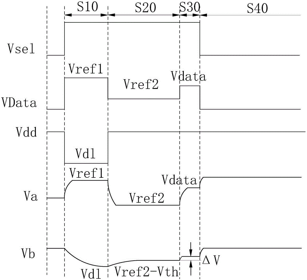
[0059] In order to further illustrate the technical means adopted by the present invention and its effects, the following describes in detail in conjunction with preferred embodiments of the present invention and accompanying drawings.

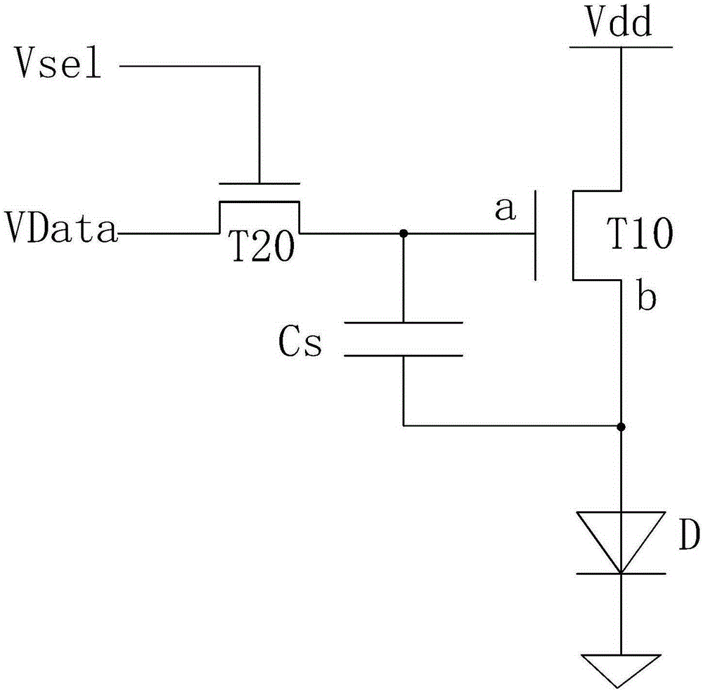
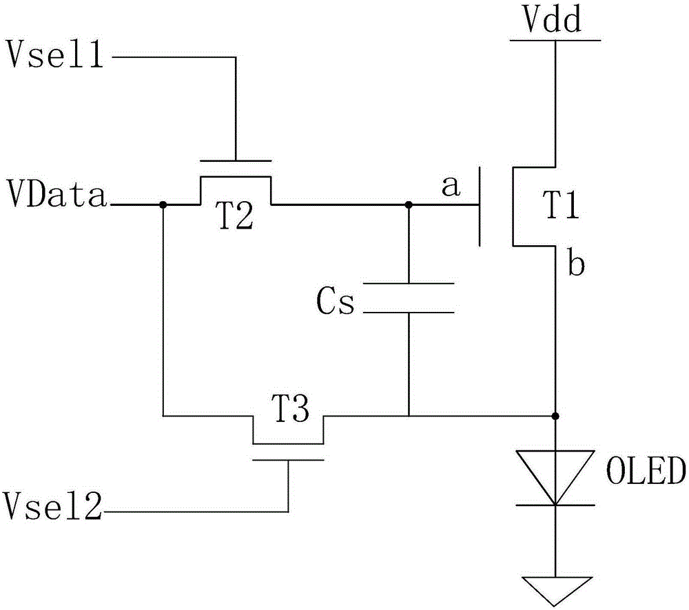
[0060] see image 3 , The present invention firstly provides an AMOLED pixel driving circuit, including: a first thin film transistor T1, a second thin film transistor T2, a third thin film transistor T3, a storage capacitor Cs, and an organic light emitting diode OLED.

[0061] The gate of the first thin film transistor T1 is electrically connected to the first node a, the source is electrically connected to the second node b, and the drain is electrically connected to the power supply voltage Vdd;

[0062] The gate of the second thin film transistor T2 is electrically connected to the first scanning signal voltage Vsel1, the source is electrically connected to the data signal voltage VData, and the drain is electrically connected to the firs...


PUM


Abstract

The invention provides an AMOLED pixel driving circuit and a pixel driving method. The AMOLED pixel driving circuit adopts a 3T1C structure and comprises a first thin film transistor (T1), a second thin film transistor (T2), a third thin film transistor (T3), a storage capacitor (Cs) and an organic light emitting diode ( OLED). A second scanning signal voltage (Vsel2) is introduced. The third thin film transistor (T3) provides an initial low potential (Vini) of a data signal voltage (VData) for the first thin film transistor (T1) which is a source electrode driving the thin film transistors at a reset phase so that a threshold voltage change driving the thin film transistors can be effectively compensated and a complexity of a power supply voltage signal is reduced.

Description

technical field [0001] The invention relates to the field of display technology, in particular to an AMOLED pixel driving circuit and a pixel driving method. Background technique [0002] Organic light emitting diode (Organic Light Emitting Display, OLED) display device has self-illumination, low driving voltage, high luminous efficiency, short response time, high definition and contrast, nearly 180° viewing angle, wide operating temperature range, and can realize flexible display and large-area comprehensive display. With many advantages such as color display, it is recognized by the industry as the display device with the most development potential. [0003] OLED display devices can be divided into two categories: passive matrix OLED (PassiveMatrixOLED, PMOLED) and active matrix OLED (ActiveMatrixOLED, AMOLED) according to the driving method, namely direct addressing and thin film transistor (ThinFilmTransistor, TFT) matrix addressing. kind. Among them, AMOLED has pixels...

Claims


Application Information

Patent Timeline
Patent Type & Authority Applications(China)
IPC IPC(8): G09G3/32
CPCG09G3/3233G09G2300/0842G09G2300/0819H10K59/131H10K59/1213G09G3/3258G09G3/3266G09G3/3291G09G2330/021H01L27/1225H01L27/124H01L27/1255
Inventor 蔡玉莹
Owner TCL CHINA STAR OPTOELECTRONICS TECH CO LTD
Why Eureka
Try Eureka