Nitride-based light emitting diode chip and manufacturing method thereof

A light-emitting diode, gallium nitride-based technology, used in laser welding equipment, manufacturing tools, welding equipment, etc., can solve the problems of difficult to spontaneously eliminate, affect luminous efficiency, light absorption, etc., to improve the overall luminous efficiency and improve light output. Efficiency, increase the effect of side wall light

Active Publication Date: 2015-12-23
XIAMEN SANAN OPTOELECTRONICS TECH CO LTD
View PDF3 Cites 3 Cited by
  • Summary
  • Abstract
  • Description
  • Claims
  • Application Information

AI Technical Summary

Problems solved by technology

However, by-products such as burn marks and debris left after laser stealth cutting in this invention are located inside the device, and are not easy to be eliminated

Method used


Image

  • Nitride-based light emitting diode chip and manufacturing method thereof
  • Nitride-based light emitting diode chip and manufacturing method thereof
  • Nitride-based light emitting diode chip and manufacturing method thereof

Examples


Example Embodiment

[0025] Example 1

[0026] This embodiment provides a preparation method of a gallium nitride light emitting diode chip, and the preparation steps include:

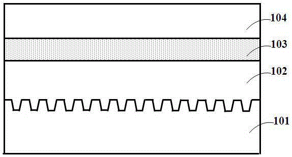
[0027] like figure 1 As shown, metal-organic chemical vapor deposition (MOCVD) is used to epitaxially grow on the patterned sapphire substrate 101 in sequence: an N-GaN layer 102 , a light-emitting layer 103 , and a P-GaN layer 104 .

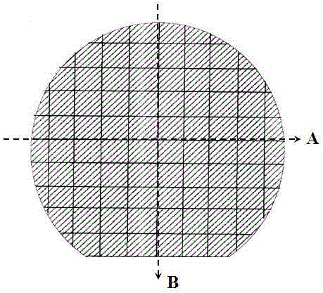
[0028] like figure 2 As shown in the figure, laser scribing is performed along the surface of the epitaxial layer, a longitudinal straight line B is formed in the direction perpendicular to the flat edge, and a transverse straight line A is formed in the direction parallel to the flat edge, and the lines A and B form a network structure. cutting path.

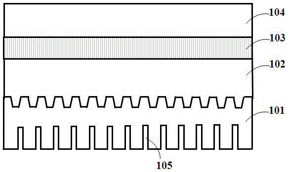
[0029] like image 3 As shown, the laser stealth cutting is used to focus at a position of 10μm~40μm inward from the back of the substrate, the laser energy is adjusted to 0.32W~0.6W, the laser frequency is adjusted to 15KHz~40KHz, an...

Example Embodiment

[0032] Example 2

[0033] like Figure 5 As shown, what is different from Embodiment 1 is that this embodiment is provided with a distributed Bragg reflection layer 108 on the backside of the substrate, so that the light extraction efficiency of the light emitting diode chip is further improved. It should be noted that the DBR 108 can be prepared before the ablation holes are obtained by laser stealth cutting inside the substrate, or can be formed after the ablation holes are obtained by laser stealth cutting inside the substrate.


PUM

PropertyMeasurementUnit
Spacingaaaaaaaaaa

Abstract

The invention provides a nitride-based light emitting diode chip and a manufacturing method thereof. Focusing at a position having a distance of 10mum-40mum to a back face of a substrate inwards is carried out, laser energy increases, laser frequency is adjusted, hidden laser cutting is realized in the substrate to form a hole through ablation penetrating through the back face of the exposed substrate, accessory substances such as burn marks and chippings generated during hidden laser cutting are effectively discharged, light absorption of the accessory substances can be reduced, light emission at side walls of the light emitting diode increases, and light emitting efficiency is improved, moreover, as the substrate and the hole have different refractive indexes, and laser scratch makes side faces of an LED chip coarsen similarly, a light removal angle is improved, increase of axial light is realized, and integral light emitting efficiency of the LED chip is improved.

Description

technical field [0001] The invention relates to the field of preparation of semiconductor devices, in particular to a gallium nitride-based light-emitting diode chip and a preparation method thereof. Background technique [0002] At present, gallium nitride-based light-emitting diode chips (Light Emitting Diode, referred to as LED in English) have excellent characteristics such as long life, impact resistance, shock resistance, high efficiency and energy saving, and are widely used in image display, signal indication, lighting and basic research. GaN-based LEDs have developed rapidly in recent years, but their luminous efficiency has always been the main bottleneck restricting the wide application of LEDs in the lighting field. For this reason, the research on improving LED luminous efficiency is relatively active. The main technologies include surface (interface) roughening technology, growth distribution Bragg reflective layer structure, transparent substrate technology, s...

Claims


Application Information

Patent Timeline
IPC IPC(8): H01L21/78H01L21/268H01L33/00B23K26/36
CPCB23K26/361H01L21/268H01L21/78H01L33/0066H01L33/0075
Inventor 陈功林素慧张家宏彭康伟许圣贤刘传桂林潇雄
Owner XIAMEN SANAN OPTOELECTRONICS TECH CO LTD
Why Eureka
Try Eureka