ESD protecting unit, array base plate, liquid crystal display panel and display device

An ESD protection and array substrate technology, applied in transistors, electrical components, optics, etc., can solve problems such as poor ESD protection effect, reduce the probability of breakdown, solve the problem of poor ESD protection effect, and reduce the effect of voltage drop

Active Publication Date: 2015-12-30
BOE TECH GRP CO LTD
View PDF6 Cites 1 Cited by
  • Summary
  • Abstract
  • Description
  • Claims
  • Application Information

AI Technical Summary

Problems solved by technology

[0004] The object of the present invention is to provide an ESD protection unit, an array substrate, a liquid crystal panel and a display device, so as to solve the problem of poor ESD protection effect in the preparation process of the array substrate

Method used


Image

  • ESD protecting unit, array base plate, liquid crystal display panel and display device
  • ESD protecting unit, array base plate, liquid crystal display panel and display device

Examples


Embodiment Construction

[0023] In order to further illustrate the ESD protection unit, the array substrate, the liquid crystal panel and the display device provided by the embodiments of the present invention, a detailed description will be given below in conjunction with the accompanying drawings.

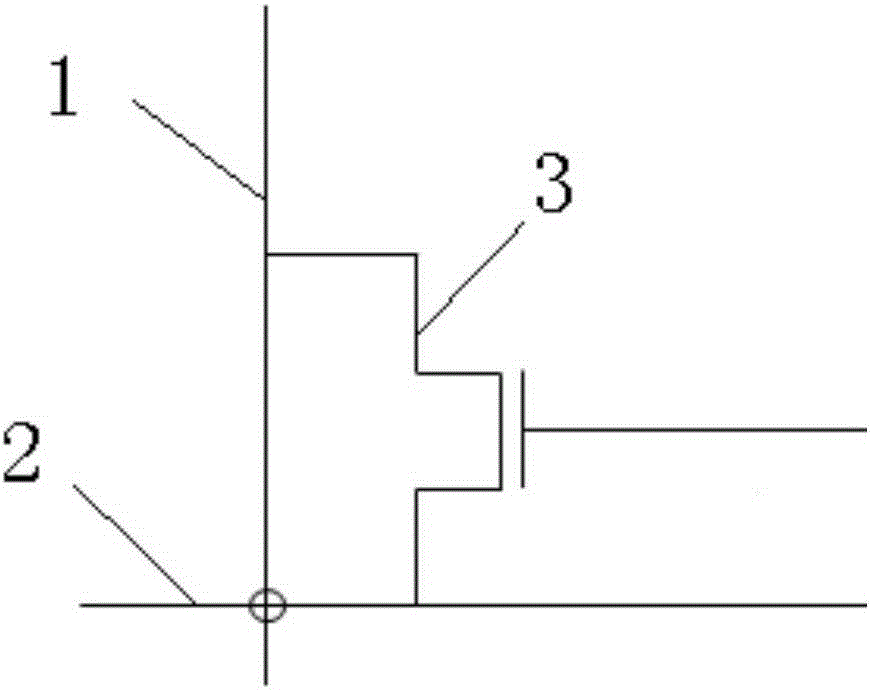
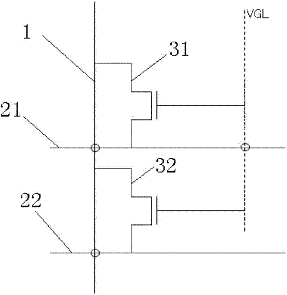
[0024] see figure 1 , the ESD protection unit provided by the embodiment of the present invention includes a thin film transistor 3, a first lead 1 and a second lead 2, and there is a voltage difference between the first lead 1 and the second lead 2; wherein, the source of the thin film transistor is connected to the second lead 2 One lead is connected, the drain of the thin film transistor is connected to the second lead, and the gate surface of the thin film transistor is exposed in the area corresponding to the pixel unit formed between the first lead 1 and the second lead 2, so as to collect the first lead 1 and the charge generated between the second lead 2.

[0025] Moreover, whether the first lea...


PUM


Abstract

The invention discloses an ESD (Electronic Static Discharge) protecting unit, an array base plate, a liquid crystal display panel and a display device and belongs to the technical field of liquid crystal display. The invention aims to solve the problem of poor ESD protecting effect during a preparation process of the array base plate. The ESD protecting unit comprises a thin film transistor, a gate line and a data line, wherein a grid electrode of the thin film transistor is exposed in an area formed by the data line and the gate line; a source electrode of the thin film transistor is connected with the data line; a drain electrode of the thin film transistor is connected with the gate line; or the source electrode of the thin film transistor is connected with the gate line and the drain electrode of the thin film transistor is connected with the data line. The liquid crystal display panel comprises the array base plate containing the ESD protecting unit, wherein the drain electrode of the thin film transistor is connected with a direct current negative voltage source in each ESD protecting unit. The ESD protecting unit provided by the invention is applicable to the display device.

Description

technical field [0001] The invention relates to the technical field of liquid crystal display, in particular to an ESD protection unit, an array substrate, a liquid crystal panel and a display device. Background technique [0002] At present, the manufacturing process of liquid crystal panels mainly includes three processes: array substrate manufacturing process, liquid crystal cell manufacturing process and module assembly process. Among them, in the array substrate preparation process, due to the need to continuously transfer the glass substrate and prepare thin film transistors on the glass substrate; therefore, the glass substrate will be constantly rubbed and moved during the process of transferring the glass substrate and preparing thin film transistors on the glass substrate , so as to continuously generate static electricity; moreover, since the glass substrate is an insulator, the static electricity generated in the array substrate preparation process is slow to dis...

Claims


Application Information

Patent Timeline
Patent Type & Authority Applications(China)
IPC IPC(8): G02F1/1362G02F1/1368
CPCG02F1/136204G02F1/1368G02F1/13685H01L27/0266H01L27/0292G02F1/134309G02F1/136259G02F1/136286G02F1/136263H01L27/0288H01L27/1244H01L27/1259
Inventor 曹昆
Owner BOE TECH GRP CO LTD
Why Eureka
Try Eureka