A kind of array substrate and its preparation method, display panel

A technology for array substrates and substrate substrates, applied in the direction of instruments, semiconductor devices, electrical components, etc., can solve the problems of lower backlight transmittance, etc., and achieve the effects of improving backlight transmittance, reducing shading, and reducing the impact of brightness

Inactive Publication Date: 2018-03-30
BOE TECH GRP CO LTD +1
View PDF5 Cites 0 Cited by
  • Summary
  • Abstract
  • Description
  • Claims
  • Application Information

AI Technical Summary

Problems solved by technology

[0005] The object of the present invention is to provide an array substrate and its preparation method, and a display panel, so as to solve the problem that in the array substrate prepared by the prior art, pixel electrodes and common electrodes are made on the upper surface of the base substrate, resulting in a decrease in backlight transmittance

Method used


Image

  • A kind of array substrate and its preparation method, display panel
  • A kind of array substrate and its preparation method, display panel
  • A kind of array substrate and its preparation method, display panel

Examples


Embodiment Construction

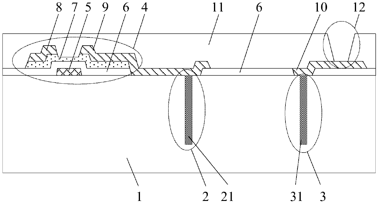
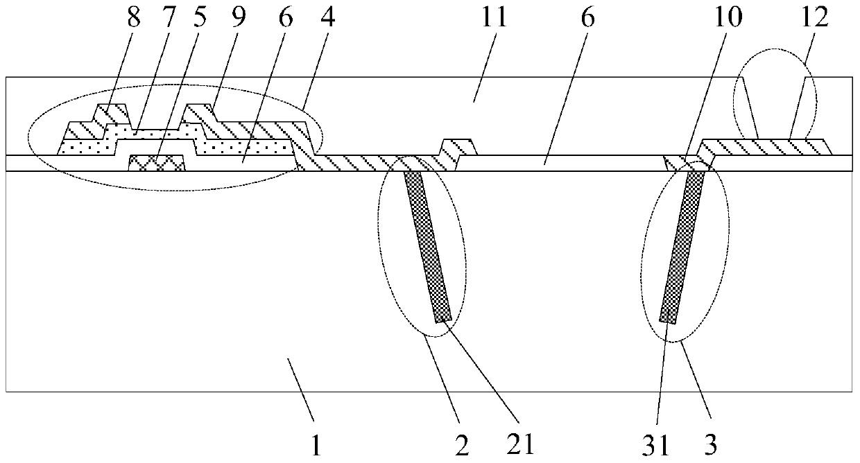
[0048] The implementation process of the embodiment of the present invention will be described in detail below in conjunction with the accompanying drawings. It should be noted that the same or similar reference numerals represent the same or similar elements or elements having the same or similar functions throughout. The embodiments described below by referring to the figures are exemplary only for explaining the present invention and should not be construed as limiting the present invention.

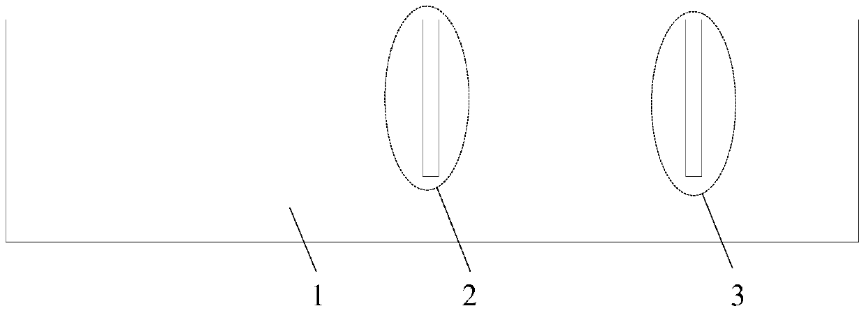
[0049] see Figure 1 to Figure 4 , the embodiment of the present invention provides an array substrate, including a base substrate 1, a plurality of pixel units arranged on the upper surface of the base substrate 1, the pixel units are arranged in an array on the base substrate 1; the upper surface of the base substrate 1 The surface is formed with a first electrode groove 2 and a second electrode groove 3 corresponding to each pixel unit, and the first electrode groove 2 and the sec...


PUM


Abstract

The invention discloses an array substrate, a preparation method thereof, and a display panel, in order to solve the problem that in the array substrate prepared by the prior art, pixel electrodes and common electrodes composed of translucent metal film layers parallel to the base substrate reduce the backlight transmittance , A problem that affects the brightness of TFT-LCD. The array substrate includes a base substrate, a plurality of pixel units arranged on the upper surface of the base substrate, and the pixel units are arranged in an array on the base substrate; corresponding The first electrode groove and the second electrode groove of each pixel unit, the first electrode groove and the second electrode groove extend from the upper surface to the lower surface of the base substrate; the pixel unit It includes a pixel electrode and a common electrode, the pixel electrode is formed in the first electrode groove, and the common electrode is formed in the second electrode groove.

Description

technical field [0001] The invention relates to the field of liquid crystal display, in particular to an array substrate, a preparation method thereof, and a display panel. Background technique [0002] Thin Film Transistor Liquid Crystal Display (TFT-LCD) has the characteristics of small size, low power consumption, no radiation, and relatively low manufacturing cost, and occupies a dominant position in the current flat panel display market. [0003] The main structure of TFT-LCD includes an array substrate and a color filter substrate that are boxed together and liquid crystals are sandwiched between them. On the array substrate, gate lines that provide scanning signals, data lines that provide data signals, and pixel electrodes that form pixel points are formed. . In order to realize the display function, it is also necessary to set a common electrode, so that when the power is applied, the liquid crystal will rotate under the action of the electric field formed by the c...

Claims


Application Information

Patent Timeline
Patent Type & Authority Patents(China)
IPC IPC(8): H01L27/12
CPCG02F1/134363G02F1/13439G02F1/1368G02F2201/121G02F2201/123G02F1/136227G02F2201/124G02F1/136222
Inventor 张颖侯智吴代吾杨子衡王轶南丁欣陈甫刘建辉沈镕
Owner BOE TECH GRP CO LTD
Why Eureka
Try Eureka