Conductive patterns and electrode patterns for single-layer capacitive touch screens
A conductive pattern, single-layer technology, applied to conductive layers on insulating carriers, electrical digital data processing, input/output processes of data processing, etc. Low visibility effects
- Summary
- Abstract
- Description
- Claims
- Application Information
AI Technical Summary
Problems solved by technology
Method used
Image

Examples
Embodiment Construction
[0048] Hereinafter, when the present invention will be described in detail, it will be described with reference to the accompanying drawings. However, it goes without saying that the present invention can be variously modified and modified without departing from the technical scope thereof, and is not limited by the following embodiments. limited.
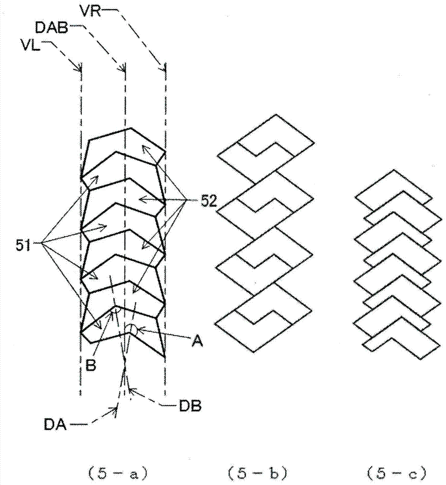
[0049] image 3 It is a diagram illustrating a unit pattern used in the conductive pattern of the present invention, and the parts drawn by lines (excluding lines, arrows, symbols, etc. for description) are thin metal lines. The unit figure of the present invention is a figure selected from the following figures: as an interior angle, there is an angle (A angle) greater than 180° and 5 angles less than 180°, A angle and the third angle counted downward from A angle The sum of the angles of (B angle) is a concave hexagon of 360° and its congruent figures. image 3 In (3-a), angle A is greater than 180°, and the other five angles are...
PUM
| Property | Measurement | Unit |
|---|---|---|
| length | aaaaa | aaaaa |
Abstract
Description
Claims
Application Information
 - R&D
- Intellectual Property
- Life Sciences
- Materials
- Tech Scout
- Unparalleled Data Quality
- Higher Quality Content
- 60% Fewer Hallucinations
Browse by: Latest US Patents, China's latest patents, Technical Efficacy Thesaurus, Application Domain, Technology Topic, Popular Technical Reports.
© 2025 PatSnap. All rights reserved.Legal|Privacy policy|Modern Slavery Act Transparency Statement|Sitemap|About US| Contact US: help@patsnap.com