Microwave communication device cavity and microwave communication device

A microwave communication and cavity technology, applied in waveguide devices, electrical components, circuits, etc., can solve problems such as solder loss, unsightly appearance, and influence on welding quality, so as to slow down heat dissipation, speed up welding speed, and improve welding quality Effect

Active Publication Date: 2018-09-25
COMBA TELECOM TECH (GUANGZHOU) CO LTD
View PDF7 Cites 0 Cited by
  • Summary
  • Abstract
  • Description
  • Claims
  • Application Information

AI Technical Summary

Problems solved by technology

However, in existing microwave communication devices, there is no structure for fixing cables on the cavity, and the welding position between the cable and the cavity cannot be accurately positioned, which leads to poor welding effect and poor welding consistency of the microwave communication device.
[0003] At the same time, during the welding process between the cavity and the outer conductor, the solder flows around, which causes the heat of the solder to lose rapidly and affects the welding quality, and causes poor consistency and unsightly appearance due to the solder flowing around.

Method used


Image

  • Microwave communication device cavity and microwave communication device
  • Microwave communication device cavity and microwave communication device

Examples


Embodiment Construction

[0016] The present invention will be further described below with reference to the accompanying drawings and exemplary embodiments, wherein the same reference numerals in the accompanying drawings all refer to the same components. Also, detailed descriptions of known arts will be omitted if they are unnecessary to illustrate the features of the present invention.

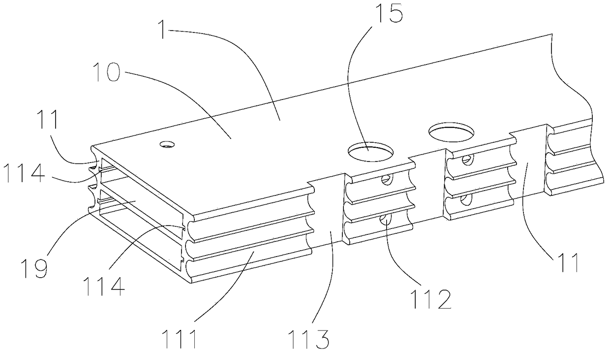
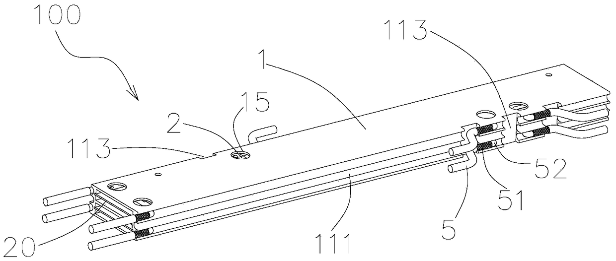
[0017] figure 1 The microwave communication device cavity 1 (hereinafter referred to as "cavity") of the present invention is shown; figure 2 shows the microwave communication device 100 of the present invention, which applies figure 1 Chamber 1 shown, figure 2 At the same time, the installation relationship between the cavity and the cable 5 is shown.

[0018] The microwave communication device 100 includes a cavity 1 , a microwave communication circuit 2 and a medium (not shown) all disposed in the cavity 1 .

[0019] The cavity 1 is a metal cavity, which includes a bottom wall 19, a pair of side walls 11 ex...


PUM


Abstract

The invention discloses a cavity of a microwave communication device. At least one of two transverse ends of the cavity is open; the cavity comprises a bottom wall, a pair of side walls extending upwards on two sides in the longitudinal direction of the bottom wall and a top wall spanning the pair of side walls; the top wall, the bottom wall and the pair of side walls jointly define a cavity for accommodating a microwave communication circuit and a medium; a wiring groove for paving an outer conductor of a cable therein is formed in at least one side wall, a yielding hole which penetrates through the side wall of the cavity and allows an inner conductor of the cable and the medium to pass is formed in the wiring groove, and the cavity is provided with a heat resistant slot for cutting off the wiring groove in at least one of the left and right sides of the yielding hole. The cavity facilitates positioning and welding of the cable, and ensures high welding quality and good consistency. The invention further discloses a microwave communication device adopting the cavity.

Description

【Technical field】 [0001] The invention relates to the technical field of microwave communication, in particular to a microwave communication device cavity and the microwave communication device. 【Background technique】 [0002] In existing microwave communication devices, the outer conductor of the cable is welded to the cavity to form a circuit loop with the inner conductor and the microwave communication circuit, and the outer conductor can also play a certain shielding role. However, in the existing microwave communication device, there is no structure for fixing the cable on the cavity, and the welding position between the cable and the cavity cannot be accurately positioned, which leads to poor welding effect and poor welding consistency of the microwave communication device. [0003] At the same time, during the welding process between the cavity and the outer conductor, the solder flows around, which causes the heat of the solder to be lost rapidly and affects the weld...

Claims


Application Information

Patent Timeline
Patent Type & Authority Patents(China)
IPC IPC(8): H01P1/04
Inventor 刘培涛陈礼涛苏国生孙善球
Owner COMBA TELECOM TECH (GUANGZHOU) CO LTD
Why Eureka
Try Eureka