Travelling wave structure photo-detector chip and preparation method thereof

A traveling wave structure, photodetector technology, applied in the directions of instruments, optics, light guides, etc., can solve the problems of radio frequency transmission line unfavorable radio frequency signal transmission, increase the effective mode coefficient of the transmission line, affect the photoelectric conversion efficiency and other problems, and achieve a high application prospect, Easy-to-process, highly responsive effects

Active Publication Date: 2016-01-20
SUN YAT SEN UNIV
View PDF6 Cites 4 Cited by
  • Summary
  • Abstract
  • Description
  • Claims
  • Application Information

AI Technical Summary

Problems solved by technology

The rotation of the transmission line can achieve better speed matching, but there are also certain problems, such as the angle between the wave vector of the optical signal and the wave vector of the radio frequency signal, which affects the efficiency of photoelectric conversion
Moreover, the layout of the rotating transmission line is confusing, which is not conducive to the high integration on the chip
In addition, there is also a

Method used


Image

  • Travelling wave structure photo-detector chip and preparation method thereof
  • Travelling wave structure photo-detector chip and preparation method thereof
  • Travelling wave structure photo-detector chip and preparation method thereof

Examples


Embodiment Construction

[0024] The drawings are for illustrative purposes only, and should not be construed as limitations on this patent; in order to better illustrate this embodiment, some parts in the drawings will be omitted, enlarged or reduced, and do not represent the size of the actual product;

[0025] For those skilled in the art, it is understandable that some well-known structures and descriptions thereof may be omitted in the drawings. The technical solutions of the present invention will be further described below in conjunction with the accompanying drawings and embodiments.

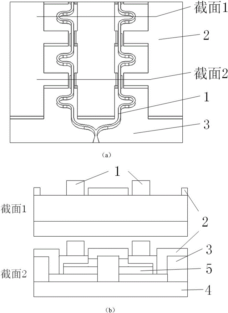
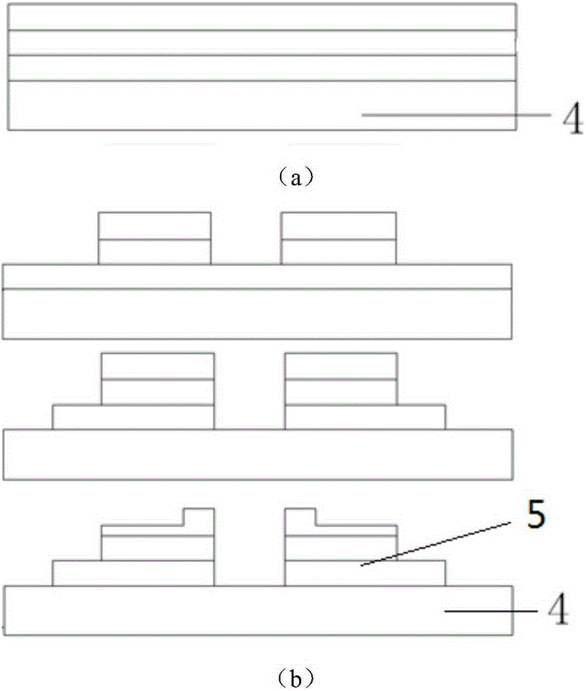
[0026] figure 1 (a) is the overall structural diagram of the detector chip of the present invention, figure 1 (b) is a schematic diagram of the corresponding cross section, where 1 is the optical waveguide, 2 is the metal electrode, 3 is the dielectric buffer layer, 4 is the chip substrate, and 5 is the photodiode unit.

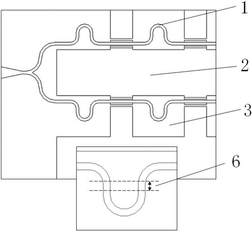
[0027] figure 2 It is a schematic diagram of the curved waveguide in the present inventi...


PUM

PropertyMeasurementUnit
Widthaaaaaaaaaa
Thicknessaaaaaaaaaa

Abstract

The invention relates to a travelling wave structure photo-detector chip and a preparation method thereof. A travelling wave structure photo-detector serves as a framework of RF coplanar waveguide transmission lines based on broadband impedance match, and is used to collect and transmit RF electromagnetic wave signals generated by photodiode units. On the basis that the basic electrode structure of the RF transmission lines are not damaged, the multiple photodiode units are connected in serial and loaded between dielectric media at the two sides of the RF transmission line to realize coherent stack of the RF signals and improve the response degree of the photo-detector. Optical signals are transmitted via optical waveguide of multi-bending at the two sides, and fed to the photodiode unit in the evanescent wave coupling mode, and the optical signals are absorbed and converted in high efficiency. The light path is controllable via the multi-bending waveguide, the speed of the waveguide transmission group is reduced to match the speed of the transmission phase of the transmission line, destructive interference is prevented from leading to reflection of RF signals, and the integral bandwidth of the photo-detector is not influenced.

Description

technical field [0001] The invention relates to the field of high-speed semiconductor optoelectronic devices for communication applications, and relates to a traveling wave structured light detector based on a radio frequency coplanar waveguide transmission line frame with broadband impedance matching and a preparation method. Background technique [0002] According to Shannon's information theory, under a constant signal-to-noise ratio, the information capacity of an analog channel is proportional to the frequency bandwidth of electromagnetic waves; broadband detectors are indispensable for greatly improving communication capacity. For traditional surface-incidence photodetectors, due to the broadband requirement, the intrinsic absorption layer of the photodiode needs to be as thin as possible to reduce the bandwidth limitation of the device due to the carrier transition. However, the thinnest possible absorbing layer weakens the absorption of the optical signal, making the...

Claims


Application Information

Patent Timeline
IPC IPC(8): H01L31/10H01L31/105G02B6/122H01L31/18
CPCG02B6/122H01L31/10H01L31/105H01L31/18
Inventor 陈钰杰许鹏飞余思远张彦峰刘洁
Owner SUN YAT SEN UNIV
Why Eureka
Try Eureka