Method for detecting circuit board based on three-dimensional characteristics

A technology of three-dimensional features and detection methods, which is applied in the field of optical detection, can solve problems such as strength reduction and impedance change, and achieve the effect of accurate blind hole quality detection

Active Publication Date: 2016-01-27
BEIJING LUSTER LIGHTTECH
View PDF6 Cites 3 Cited by
  • Summary
  • Abstract
  • Description
  • Claims
  • Application Information

AI Technical Summary

Problems solved by technology

This kind of defect will lead to a decrease in intensity or even a change in impedance, which needs to be detected, but the

Method used


Image

  • Method for detecting circuit board based on three-dimensional characteristics
  • Method for detecting circuit board based on three-dimensional characteristics
  • Method for detecting circuit board based on three-dimensional characteristics

Examples


Example Embodiment

[0041] In order to enable those skilled in the art to better understand the technical solutions in the present invention, the following will clearly and completely describe the technical solutions in the embodiments of the present invention with reference to the accompanying drawings in the embodiments of the present invention. Obviously, the described The embodiments are only a part of the embodiments of the present invention, rather than all the embodiments. Based on the embodiments of the present invention, all other embodiments obtained by those of ordinary skill in the art without creative work shall fall within the protection scope of the present invention.

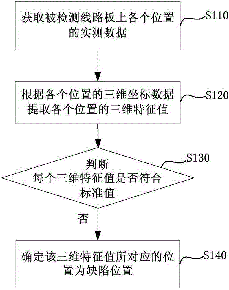
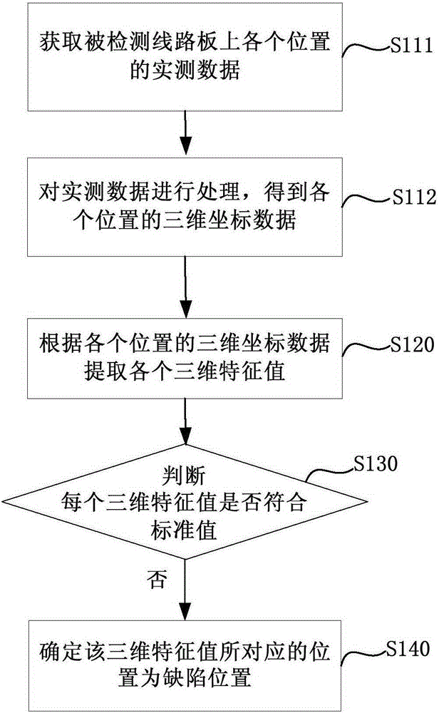
[0042] The invention provides a circuit board detection method based on three-dimensional features, such as figure 1 As shown, the method includes:

[0043] Step S110: Acquire three-dimensional coordinate data of various positions on the detected circuit board, where the three-dimensional coordinate data includes X-axis ...


PUM


Abstract

The invention discloses a method for detecting a circuit board based on three-dimensional characteristics. The method comprises the following steps: acquiring three-dimensional coordinate data on each position of the detected circuit board; extracting each three-dimensional characteristic value according to the three-dimensional coordinate data on each position; judging if each three-dimensional characteristic value meets a standard value; and when the three-dimensional characteristic value does not meet the standard value, confirming the position corresponding to the three-dimensional characteristic value as a defect position. According to the scheme, the three-dimensional coordinate data on each point of the circuit board is collected, treated, compared and analyzed, so that the detecting result is acquired and the defects of all the circuit boards can be detected; the method is not influenced by the environments of oxidation, smudge, and the like; the false detecting rate or false reporting rate caused by the environmental influence is effectively reduced; besides, the sunken defect and the blind hole which cannot be detected by a traditional automatic optical detector can be detected.

Description

technical field [0001] The invention relates to the technical field of optical detection, in particular to a circuit board detection method based on three-dimensional features. Background technique [0002] Printed circuit board (PCB, PrintedCircuitBoard) is the substrate for assembling electronic parts and the key electrical interconnection of electronic products. It is called "the mother of electronic system products". The inspection of printed circuit boards is realized by automatic optical inspection instrument (AOI). [0003] In the process of automatic optical inspection instrument testing printed circuit boards, the existing inspection method is to first obtain the plane image of the product, then compare the plane image with the standard image, and then judge the defect of the inspected product according to the comparison result . Specifically, from the perspective of detecting the features used, existing methods are based on "grayscale features of planar images". ...

Claims


Application Information

Patent Timeline
IPC IPC(8): G01N21/88
Inventor 金刚姚毅刘朝朋
Owner BEIJING LUSTER LIGHTTECH
Why Eureka
Try Eureka