Manufacturing method of flip LED chip with enhanced anti-EOS capability

A technology of LED chip and manufacturing method, which is applied in the direction of electrical components, circuits, semiconductor devices, etc., can solve the problems of weak anti-EOS ability and thin evaporation thickness, and achieve the effect of enhancing the anti-EOS ability

Active Publication Date: 2022-03-15
JUCAN PHOTOELECTRIC TECH (SUQIAN) CO LTD
View PDF3 Cites 0 Cited by
  • Summary
  • Abstract
  • Description
  • Claims
  • Application Information

AI Technical Summary

Problems solved by technology

[0005] This application provides a method for manufacturing a flip-chip LED chip with enhanced anti-EOS ability to solve the problem that the second electrode evaporation thickness of the LED chip in the prior art is too thin and the anti-EOS ability is weak, which specifically includes the following steps:

Method used


Image

  • Manufacturing method of flip LED chip with enhanced anti-EOS capability
  • Manufacturing method of flip LED chip with enhanced anti-EOS capability

Examples


Embodiment Construction

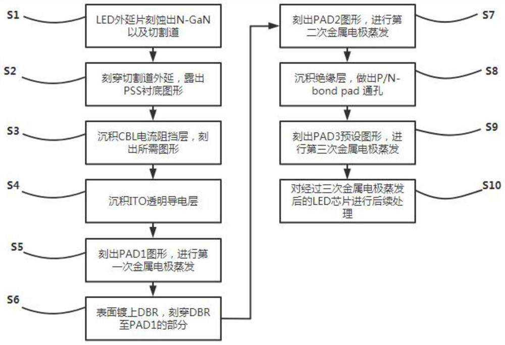
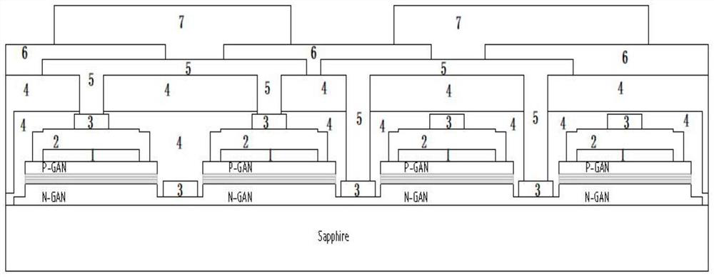
[0035] The technical solutions in the embodiments of the present invention will be clearly and completely described below in conjunction with the accompanying drawings in the embodiments of the present invention. Obviously, the described embodiments are only some, not all, embodiments of the present invention. Based on the embodiments of the present invention, all other embodiments obtained by persons of ordinary skill in the art without creative efforts fall within the protection scope of the present invention.

[0036] When manufacturing LED chips by the traditional method, because the thickness of the second evaporation of the metal electrode has little effect on the brightness, in order to save manufacturing costs, the thickness of the second evaporation of the metal electrode is controlled at 0.5-1um. Thin, easy to lead to weak anti-EOS ability, LED chips are prone to EOS events, bonding wire fusing, chip or Zener breakdown, and burnt phenomenon, reducing the service life ...


PUM

PropertyMeasurementUnit
thicknessaaaaaaaaaa
thicknessaaaaaaaaaa
refractive indexaaaaaaaaaa

Abstract

The invention discloses a manufacturing method of a flip LED chip with enhanced anti-EOS capability, and the method is characterized in that in the LED manufacturing process, the influence of the thickness of secondary electrode evaporation on the voltage brightness is not large, so that the thickness is usually selected to be 0.5-1 [mu] m in order to reduce the cost; research finds that the second electrode evaporation thickness is too small, and the anti-EOS capability is easy to be weak. According to the method provided by the invention, the anti-EOS capability of the LED chip is greatly improved, the probability of EOS events is reduced and the service life of the LED chip is prolonged under the condition that the photoelectric property is not influenced by increasing the thickness of the metal lamination of the second metal electrode evaporation.

Description

technical field [0001] The present application relates to the field of LED chip manufacturing, in particular to a method for manufacturing a flip-chip LED chip with enhanced anti-EOS capability. Background technique [0002] LED, also known as light-emitting diode, is a commonly used light-emitting device. LED has the characteristics of energy saving, environmental protection, safety, long life, low power consumption, etc., and can be widely used in various indications, displays, decorations, backlights, general lighting and other fields. EOS: Electrical Over Stress refers to the process in which an object is exposed to current or voltage beyond its maximum upper limit. Applied current to an LED that exceeds the maximum current specified in the LED specification beyond its maximum specified limit may result in reduced or damaged device functionality. Any EOS event may cause LED damage. This damage can manifest as an immediate failure of the LED device, such as bond wire f...

Claims


Application Information

Patent Timeline
Patent Type & Authority Applications(China)
IPC IPC(8): H01L33/14H01L33/38H01L33/46H01L33/32H01L33/00
CPCH01L33/145H01L33/38H01L33/46H01L33/32H01L33/0075Y02P70/50
Inventor 黄文光林潇雄王洪峰张振
Owner JUCAN PHOTOELECTRIC TECH (SUQIAN) CO LTD
Why Eureka
Try Eureka