Surface acoustic wave filter encapsulation structure and manufacturing method

A packaging structure, surface acoustic wave technology, applied in electrical components, impedance networks, etc., can solve problems such as functional failure, and achieve the effects of low cost, simple and easy-to-control storage methods, and easy-to-control

Active Publication Date: 2016-01-27
JCET GROUP CO LTD
View PDF6 Cites 16 Cited by
  • Summary
  • Abstract
  • Description
  • Claims
  • Application Information

AI Technical Summary

Problems solved by technology

[0008] The technical problem to be solved by the present invention is to provide a surface acoustic wave filter packaging structure and manufacturing method for the above-mentioned prior art, which uses a plastic sealing material to sea

Method used


Image

  • Surface acoustic wave filter encapsulation structure and manufacturing method
  • Surface acoustic wave filter encapsulation structure and manufacturing method
  • Surface acoustic wave filter encapsulation structure and manufacturing method

Examples


Example Embodiment

[0038] Example 1:

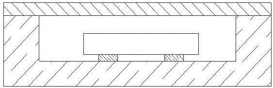
[0039] like image 3 As shown, a surface acoustic wave filter packaging structure in this embodiment includes a substrate 1, a groove 8 is provided on the front of the substrate 1, a pad 2 is provided in the groove 8, and a pad 2 is provided in the pad 2 is flip-mounted with a filter chip 3 through a conductive bump 4, and a layer of molding compound 6 is provided on the front of the substrate 1, and a protective cavity is formed between the molding compound 6 and the groove 8, and the molding compound 6 and the filter The chip functional area 3a of the chip 3 is not in contact.

[0040] The molding compound 6 is a thermosetting material, which is powder at room temperature and liquid at the melting point. The molding compound is filled to a certain height in the groove of the substrate under high temperature and then thermosets.

[0041] Its manufacturing method is as follows:

[0042] Step 1: See Figure 2a , providing a substrate with grooves on the ...

Example Embodiment

[0046] Example 2:

[0047] like Figure 4 As shown, a surface acoustic wave filter packaging structure in this embodiment includes a substrate 1, a groove 8 is provided on the front of the substrate 1, a pad 2 is provided in the groove 8, and the pad 2. The inner area is equipped with a filter chip 3 through conductive or non-conductive glue. The front side of the filter chip 3 is connected to the pad 2 through a metal wire. A layer of plastic sealing compound 6 is provided on the front side of the substrate 1. A protective cavity is formed between the grooves 8 , and the molding compound 6 is not in contact with the chip function area 3 a of the filter chip 3 .

Example Embodiment

[0048] Example 3:

[0049] like Figure 5 As shown, the difference between embodiment 3 and embodiment 1 is that the filter chip 3 is a TSV filter chip, and the filter chip 3 is provided with through holes, and the cavity structure needs to be ensured on the front and back sides of the filter chip 3, and the plastic encapsulant 6 is not in contact with the chip function area 3a of the filter chip 3.


PUM


Abstract

The invention relates to a surface acoustic wave filter encapsulation structure and a manufacturing method, and belongs to the technical field of semiconductor encapsulation. The structure comprises a substrate (1). The back of the substrate (1) is provided with a groove (8), and a filter chip (3) is mounted uprightly or inversely in the groove (8). The front of the substrate (1) is provided with a layer of encapsulation material (6). A protection cavity is formed between the encapsulation material (6) and the groove (8). The encapsulation material (6) does not contact a chip function area (3a) of the filter chip (3). According to the surface acoustic wave filter encapsulation structure and the manufacturing method of the invention, the protection cavity is sealed by the encapsulation material, and therefore, encapsulation adhesive is effectively prevented from overflowing to the function area on the surface of the filter chip, and the problem that traditional metal cover protection function causes function failure is solved.

Description

technical field [0001] The invention relates to a packaging structure and a manufacturing method of a surface acoustic wave filter, belonging to the technical field of semiconductor packaging. Background technique [0002] Due to the product performance and design function requirements of the surface acoustic wave filter, it is necessary to ensure that the functional area of ​​the filter chip cannot touch any substance, that is, the cavity structure design. The existing surface acoustic wave filter packaging structure such as figure 1 , The filter chip is connected to the ceramic substrate through conductive bump flip-chip welding and is completely embedded in the cavity of the substrate, and the surface of the substrate is protected by a metal cover. [0003] There is following shortcoming in above-mentioned existing structure: [0004] 1. The cost of the metal cover is relatively high; [0005] 2. Strict requirements on the flatness of the ceramic substrate and metal co...

Claims


Application Information

Patent Timeline
IPC IPC(8): H03H9/64H03H3/007
Inventor 吴现伟柳燕华张超
Owner JCET GROUP CO LTD
Why Eureka
Try Eureka