Semiconductor device and manufacturing method thereof

A manufacturing method and semiconductor technology, applied in semiconductor/solid-state device manufacturing, semiconductor devices, transistors, etc., can solve problems such as high cost of SOI substrates, difficulty in meeting high device integration, and influence on device heat dissipation performance, so as to eliminate self-heating effect , Eliminate floating body effect, low cost effect

Active Publication Date: 2018-06-01
INST OF MICROELECTRONICS CHINESE ACAD OF SCI
View PDF3 Cites 0 Cited by
  • Summary
  • Abstract
  • Description
  • Claims
  • Application Information

AI Technical Summary

Problems solved by technology

However, the cost of the SOI substrate is high, and a larger device area is required to avoid the floating body effect (Floating Body Effect), which is difficult to meet the requirements of high integration of the device. In addition, due to the embedding of the silicon dioxide layer, the heat dissipation of the device Performance suffers

Method used


Image

  • Semiconductor device and manufacturing method thereof
  • Semiconductor device and manufacturing method thereof
  • Semiconductor device and manufacturing method thereof

Examples


Embodiment Construction

[0050] Embodiments of the present invention are described in detail below, examples of which are shown in the drawings, wherein the same or similar reference numerals designate the same or similar elements or elements having the same or similar functions throughout. The embodiments described below by referring to the figures are exemplary only for explaining the present invention and should not be construed as limiting the present invention.

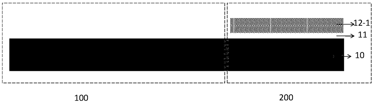
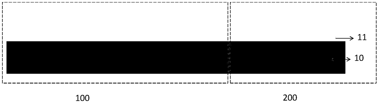
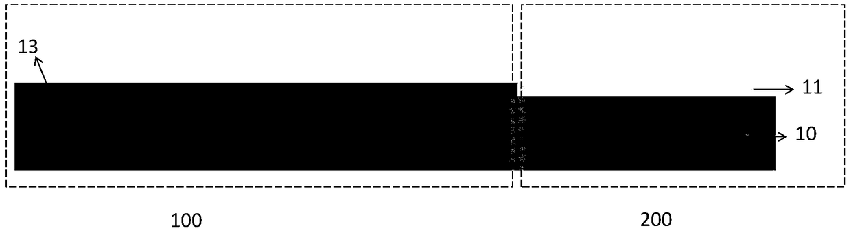
[0051] The present invention aims to propose a semiconductor device, with reference to Figure 12 , 13 As shown, the semiconductor device includes a first device region 300 and a second device region 200, wherein:

[0052] The first device region 300 includes:

[0053] a substrate 10 having a first semiconductor material;

[0054] The second semiconductor layer 13 is located on the substrate;

[0055] The third semiconductor layer 14, located on the second semiconductor layer 13, is the formation area of ​​the first device 40;

[00...


PUM


Abstract

The present invention provides a semiconductor device, comprising: a first device region and a second device region; wherein, the first device region comprises: a substrate having a first semiconductor material; a second semiconductor layer located on the substrate above; the third semiconductor layer, located on the second semiconductor layer, is the first device formation region; the first isolation structure, located on both sides of the third semiconductor layer and on the substrate; the first insulating layer, located on the third semiconductor layer Under the source and drain regions of the layer, between the first isolation structure and the end of the second semiconductor layer; the second device region includes: the substrate; the second device on the substrate; the second isolation structure, located on both sides of the second device side substrate. The device of the invention has the characteristics of low cost, small leakage, low power consumption, high speed, relatively simple process and high integration.

Description

technical field [0001] The invention relates to the field of semiconductor devices, in particular to a semiconductor device and a manufacturing method thereof. Background technique [0002] With the continuous shrinking of device size, the number of devices on a chip per unit area is increasing, which will lead to an increase in dynamic power consumption. At the same time, the continuous shrinking of device size will inevitably lead to an increase in leakage current, which in turn will cause an increase in static power consumption. , and with the high integration of semiconductor devices, the channel length of MOSFET continues to shorten, and a series of effects that can be ignored in the MOSFET long channel model become more and more significant, and even become the dominant factor affecting the performance of the device. This phenomenon is collectively referred to as short channel effect. The short channel effect will deteriorate the electrical performance of the device, ...

Claims


Application Information

Patent Timeline
Patent Type & Authority Patents(China)
IPC IPC(8): H01L27/088H01L29/78H01L29/06H01L21/8234
Inventor 许静闫江陈邦明王红丽唐波唐兆云徐烨锋李春龙杨萌萌
Owner INST OF MICROELECTRONICS CHINESE ACAD OF SCI
Why Eureka
Try Eureka