Method for preparing LEDs with different light colors based on metal nano-cluster packaging material
A technology of metal nano-clusters and packaging materials, which is applied in semiconductor devices, electrical components, circuits, etc., can solve the problems of high cost, low luminous efficiency, and restrictions on the development of LEDs, and achieve the effect of low risk and easy operation
- Summary
- Abstract
- Description
- Claims
- Application Information
AI Technical Summary
Benefits of technology
Problems solved by technology
Method used
Image
Examples
Embodiment 1
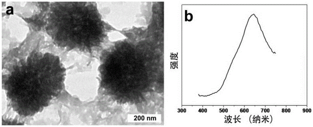
[0028] Add 5mL of 1-octadecene to a 20mL beaker, and dissolve 0.2mmol of CuCl 2 2H 2 O (the concentration of the metal precursor solution is 0.01 mol / L), under magnetic stirring at room temperature, add 1 mmol of dodecyl mercaptan dropwise and keep stirring for 3 min to obtain dodecyl mercaptan-stabilized Cu nanoclusters . Maintaining stirring at room temperature for 0.5 h, a spherical assembly structure packaging material of Cu nanoclusters with a diameter of about 200 nm can be obtained, and the spherical assembly structure packaging material of Cu nanoclusters has orange-red fluorescence. Finally, after centrifugation, drying, and powder treatment (the product is about 30 mg, the powder mesh number is 400), the Cu chip assembly structure packaging material of 5 mg is taken and blended with the prepolymer of polydimethylsiloxane of 15 mg (mass ratio It is 1:3), and then coated on the GaN-based LED chip, and polymerized at 60°C for 2 hours to obtain a packaged LED light sou...
Embodiment 2
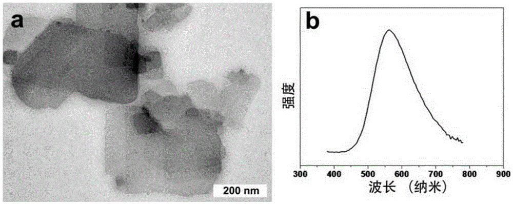
[0030] Add 5mL of 1-octadecene to a 20mL beaker, and dissolve 1.6mmol of CuCl 2 2H 2O (the concentration of the metal precursor solution is 0.08 mol / L), under magnetic stirring at room temperature, add 1 mmol of dodecyl mercaptan dropwise and keep stirring for 3 min to obtain dodecyl mercaptan-stabilized Cu nanoclusters . Stirring at room temperature for 1 hour can obtain Cu nanocluster flakes (length 50-400nm, width 50-400nm, thickness <5nm) assembly structure encapsulation material, and this Cu nanocluster flake assembly structure encapsulation material has light yellow fluorescence. Finally, through centrifugation, drying, and powder processing (about 100 mg of the product), the sheet assembly structure packaging material of the Cu nanoclusters of 5 mg is blended with the prepolymer of polydimethylsiloxane of 15 mg (mass ratio is 1: 3), and then coated on a GaN-based LED chip, and polymerized at 80° C. for 5 hours to obtain a packaged light-yellow LED light source.
Embodiment 3
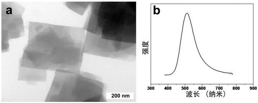
[0032] Add 5mL of 1-octadecene to a 20mL beaker, and dissolve 0.2mmol of CuCl 2 2H 2 O, under magnetic stirring at room temperature, 1 mmol of dodecyl mercaptan was added dropwise and kept stirring for 3 min to obtain dodecyl mercaptan-stabilized Cu nanoclusters. Stirring treatment at 50°C for 3 hours can obtain Cu nano-cluster thick sheet (length 100-400nm, width 100-400nm, thickness > 5nm) assembly structure packaging material, this Cu nano-cluster thick sheet assembly structure packaging material has green fluorescence. Finally, after centrifugation, drying, and powder treatment (the product is about 30 mg), take 5 mg of Cu chip assembly structure packaging material and blend it with 15 mg of polydimethylsiloxane prepolymer (mass ratio is 1:3), Then it is coated on a GaN-based LED chip and polymerized at 60° C. for 5 hours to obtain a packaged LED light source that emits green light.
PUM
| Property | Measurement | Unit |
|---|---|---|
| Diameter | aaaaa | aaaaa |
| Thickness | aaaaa | aaaaa |
Abstract
Description
Claims
Application Information


