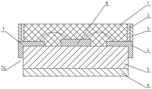
LED packaging structure
A technology for LED packaging and LED chips, applied in electrical components, circuits, semiconductor devices, etc., can solve the problems of increasing the manufacturing cost of the packaging structure, insufficient light saturation of the product, and halo of the packaging structure.
- Summary
- Abstract
- Description
- Claims
- Application Information
AI Technical Summary
Problems solved by technology
Method used
Image
Examples
Embodiment Construction
[0009] In order to make the content of the present invention more clearly understood, the present invention will be further described in detail below based on specific embodiments and in conjunction with the accompanying drawings.
[0010] Such as figure 1 As shown, an LED packaging structure includes an LED chip 8, a positive electrode sheet 7, a negative electrode sheet 4, a heat dissipation substrate 5, an encapsulating colloid 1 and a reflective cup 2, the LED chip 8 is packaged in the encapsulating colloid 1, and the LED chip 8 is connected to the positive electrode The sheet 7 is electrically connected to the negative electrode sheet 4 , the bottom surface of the LED chip 8 is against the heat dissipation substrate 5 , the encapsulant 1 is filled in the reflective cup 2 , and a light absorbing layer 3 is provided on the outside of the reflective cup 2 .
[0011] In order to improve the heat dissipation effect, a layer of silicone grease layer 6 is provided on the bottom ...
PUM
 Abstract
Description
Claims
Application Information
