Automatic test method and system of imaging chip MTF value

An automatic test system and imaging chip technology, applied in the direction of instruments, etc., can solve the problems such as MTF of the imaging chip that cannot test the photoelectric sensor, and achieve the effect of reducing human influence, simple structure and high degree of automation

Active Publication Date: 2016-03-02
LUSTER LIGHTWAVE CO LTD
View PDF11 Cites 8 Cited by
  • Summary
  • Abstract
  • Description
  • Claims
  • Application Information

AI Technical Summary

Problems solved by technology

[0006] An automatic testing method and system for the MTF value of an imaging chip is provided in an embodiment of the present invention to solve the problem in the prior art that the MTF of an imaging chip of a photoelectric sensor cannot be tested

Method used


Image

  • Automatic test method and system of imaging chip MTF value
  • Automatic test method and system of imaging chip MTF value
  • Automatic test method and system of imaging chip MTF value

Examples


Embodiment Construction

[0033] In order to enable those skilled in the art to better understand the technical solutions in the present invention, the technical solutions in the embodiments of the present invention will be clearly and completely described below in conjunction with the drawings in the embodiments of the present invention. Obviously, the described The embodiments are only some of the embodiments of the present invention, not all of them. Based on the embodiments of the present invention, all other embodiments obtained by persons of ordinary skill in the art without making creative efforts shall fall within the protection scope of the present invention.

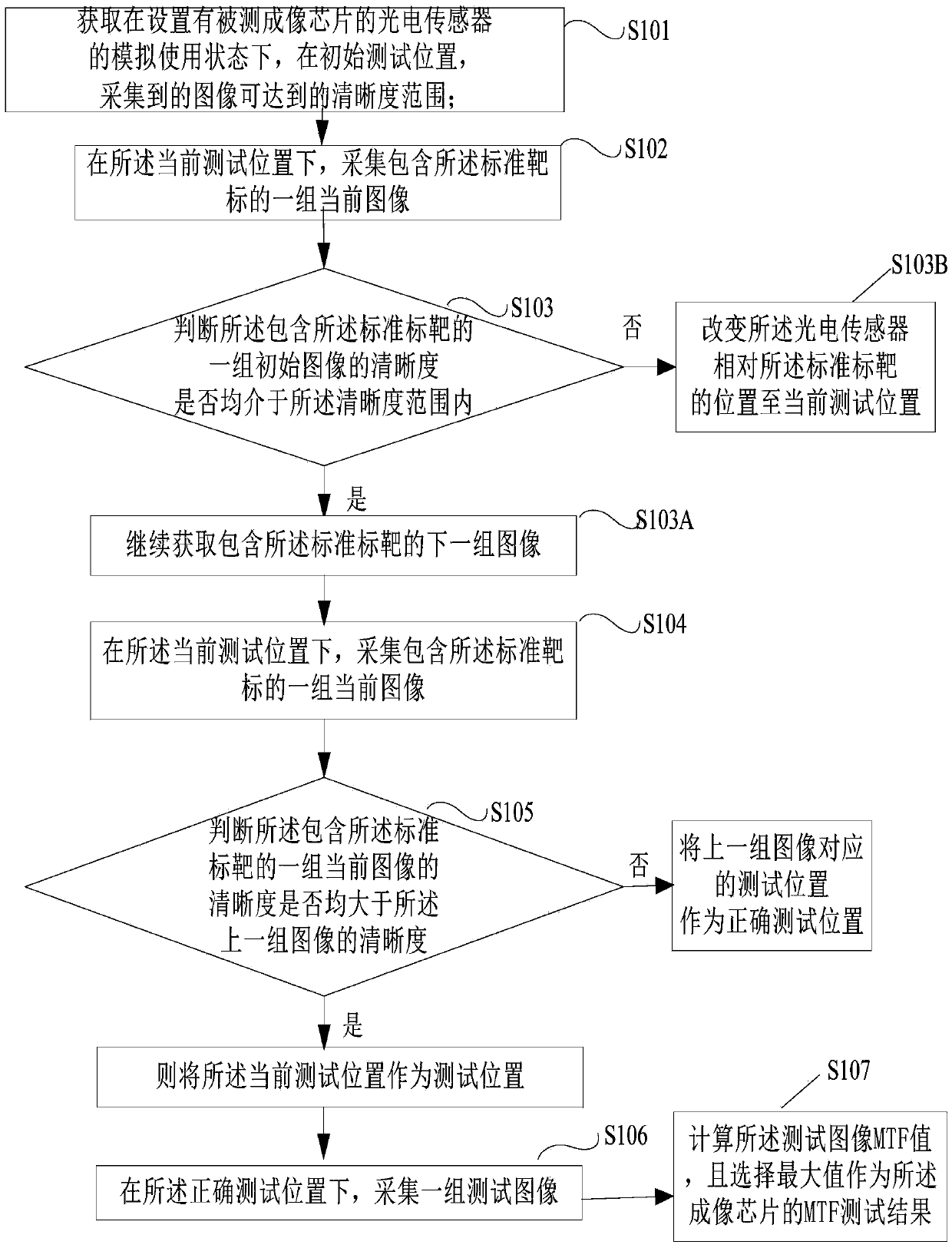
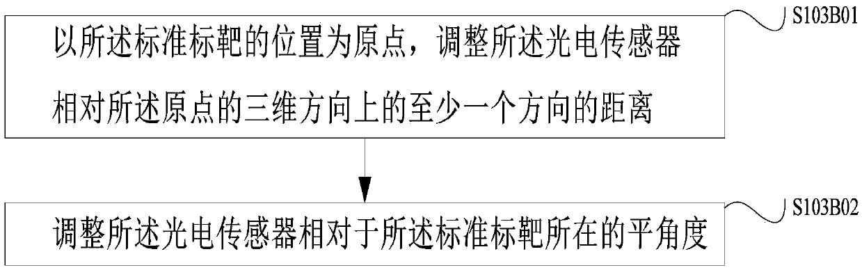
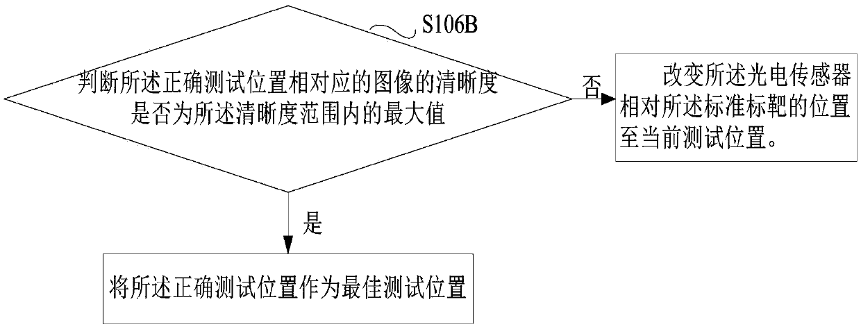
[0034] see figure 1 , is a schematic flowchart A of an automatic testing method for the MTF value of an imaging chip provided by an embodiment of the present invention. As shown in the figure, the automatic testing method includes the following steps:

[0035] In step S101 , the resolution range of the collected images at the initial ...


PUM


Abstract

The embodiment of the invention discloses an automatic test method and system of an imaging chip MTF value. The method comprises the steps of: before the test, setting an image definition range of the test; at an initial test position, collecting an initial image; judging whether the definition of the initial image is in the range, if yes, continuing to obtain a next image, and if not, changing the position of a relative standard target of a photoelectric sensor to a current test position, and then collecting a current image; judging whether the definition of the current image is larger than the last one, if yes, setting the current test position as a test position; and if not, setting the test position corresponding to the last image as a relatively good test position; and collecting test images at the relatively good test position. In addition, the invention further discloses an automatic test system and system of the imaging chip MTF value, and the system is used for realizing the above method. According to the invention, the automatic control of a position fine tuning process of a tested chip is realized, human influences in the test are reduced, and the imaging chip MTF value is tested more precisely.

Description

technical field [0001] The invention relates to the technical field of photoelectric sensor performance testing, in particular to an automatic testing method and system for the MTF value of an imaging chip. Background technique [0002] Both the optical and electrical properties of photoelectric sensors will affect its photoelectric imaging results. The photoelectric sensor is a system composed of many components, and the production and assembly relationship of each component will cause a gap between the performance of the photoelectric sensor and the target performance of the theoretical design. In the field of design, calibration evaluation and detection of photoelectric sensors, the modulation transfer function (Modulation Transfer Function, MTF for short) is often used as a parameter to judge whether the comprehensive photoelectric performance of photoelectric sensors is close to the theoretical design target. Taking a camera as an example, it is impossible to completel...

Claims


Application Information

Patent Timeline
Patent Type & Authority Applications(China)
IPC IPC(8): G01D18/00
CPCG01D18/00
Inventor 林海峰杨艺张勇
Owner LUSTER LIGHTWAVE CO LTD
Why Eureka
Try Eureka