Gate driving circuit unit and gate driving circuit
A gate drive circuit and drive circuit technology, applied in the electronic field, can solve problems such as large threshold voltage range, slow circuit operation speed, and reduced conductivity, so as to expand the adaptable range of threshold voltage, reduce rise/fall time, and speed up The effect of charging speed
- Summary
- Abstract
- Description
- Claims
- Application Information
AI Technical Summary
Problems solved by technology
Method used
Image

Examples
Embodiment 1
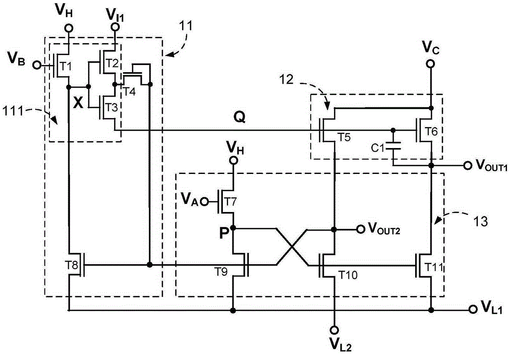
[0038] Such as figure 1 As shown, the gate drive circuit unit (that is, the shift register unit) of this embodiment includes a drive control module 11, a drive module 12, a low-level maintenance module 13, a scan signal output terminal VOUT1, a transfer signal output terminal VOUT2, and a pulse signal The input terminal VI1, the high level terminal VH, the first clock signal terminal VA, the second clock signal terminal VB, the third clock signal terminal VC, the first low level terminal VL1, and the second low level terminal VL2.
[0039] The scanning signal output terminal VOUT1 is connected to the row scanning line on the display panel, and the signal output terminal VOUT2 is used as the first pulse signal input terminal of the gate driving circuit unit of the next stage.
[0040]The drive control module 11 is connected to the pulse signal input terminal VI1, the high level terminal VH, the second clock signal input terminal VB, the drive module 12, the transmission signal ...
Embodiment 2
[0079] Such as Figure 5 As shown, the difference between this embodiment and Embodiment 1 is that the second current conduction electrode (source) of the fourth transistor T4 of the gate drive circuit unit of this embodiment receives the third clock signal input terminal VC through the third clock signal input terminal VC. clock signal, this circuit can reduce the leakage current passing through T4 and T2 from the signal output terminal VOUT2, further reducing the power consumption of the circuit. The connection mode of other modules and components in this embodiment is the same as that of the corresponding modules and components in Embodiment 1, and the principle of the working process is the same, so it will not be repeated here.
Embodiment 3
[0081] Such as Image 6 As shown, the difference between the present embodiment and the first embodiment is that the low-level maintaining module 13 of the gate driving circuit unit of the present embodiment further includes a twelfth transistor T12 and an initialization signal terminal VR. The control electrode of the twelfth transistor T12 is used to receive the initialization signal V through the initialization signal terminal VR R , its first current conduction pole is used to receive a high level through the high level terminal VH, and its second current conduction pole is connected to the control pole of the tenth transistor T10, the control pole of the eleventh transistor T11, the ninth transistor T9 The first current conduction pole, that is, the second current conduction pole thereof is connected to the sustain control terminal P.
[0082] The twelfth transistor T12 is used when the initialization signal V R When the high level comes, the maintenance control termina...
PUM
 Abstract
Description
Claims
Application Information
 - R&D
- Intellectual Property
- Life Sciences
- Materials
- Tech Scout
- Unparalleled Data Quality
- Higher Quality Content
- 60% Fewer Hallucinations
Browse by: Latest US Patents, China's latest patents, Technical Efficacy Thesaurus, Application Domain, Technology Topic, Popular Technical Reports.
© 2025 PatSnap. All rights reserved.Legal|Privacy policy|Modern Slavery Act Transparency Statement|Sitemap|About US| Contact US: help@patsnap.com