Image Display Device and Manufacturing Method for the Same

Active Publication Date: 2010-01-21
PANASONIC LIQUID CRYSTAL DISPLAY CO LTD +1
View PDF8 Cites 23 Cited by
  • Summary
  • Abstract
  • Description
  • Claims
  • Application Information

AI Technical Summary

Benefits of technology

[0014]It is therefore an object of the present invention to provide an image display device capable of suppressing leakage in a pixel TFT while being improved in driving power of a gate driver TFT, and a method of manufacturing the image display device.
[0015]A liquid crystal display device according to the present invention is capable of suppressing leakage in a pixel TFT and of improving the driving power of a gate driver TFT by forming a low mobility layer on a front side of a semiconductor film of the pixel TFT while forming no low mobility layer on a front side of a semiconductor film of the gate driver TFT, which has a dual gate structure, or selectively removing a low mobility layer from the front side of the semiconductor film of the gate driver TFT.
[0017]Alternatively, the mobility on the front side of the semiconductor film of the gate driver TFT can be made higher than the mobility on the front side of the semiconductor film of the pixel TFT by forming the TFTs in a manner that forms a source and a drain for the pixel TFT, as well as a low mobility layer on the front side of the semiconductor film of the pixel TFT, and then forms a source and a drain for the gate driver TFT, with the pixel TFT being protected. Another way to make the mobility on the front side of the semiconductor film of the gate driver TFT higher than the mobility on the front side of the semiconductor film of the pixel TFT is to form the TFTs in a manner that forms a source and a drain for the gate driver TFT, and then forms a source and a drain, as well as a low mobility layer on the semiconductor film, for the pixel TFT, with the gate driver TFT being protected.
[0028]According to the thus structured image display device and image display device manufacturing method, leakage in the pixel TFT can be suppressed and the driving power of the gate driver TFT can be improved.

Problems solved by technology

In a TFT having this structure, an influence of an electric field from the gate electrode hardly reaches a front side of the semiconductor film (herein, a top side of a semiconductor film is the front side), whereas the influence of an electric field from above often reaches the front side of the semiconductor film, resulting in a problem that leak current occurs on the front side of the semiconductor film.
However, manufacturing a polycrystalline silicon TFT requires processes that are not employed in a manufacture line for an amorphous silicon TFT, such as crystallization, impurity implantation, and activation.
Consequently, combining different characteristics required of the two TFTs has been difficult.

Method used


Image

  • Image Display Device and Manufacturing Method for the Same
  • Image Display Device and Manufacturing Method for the Same
  • Image Display Device and Manufacturing Method for the Same

Examples


second embodiment

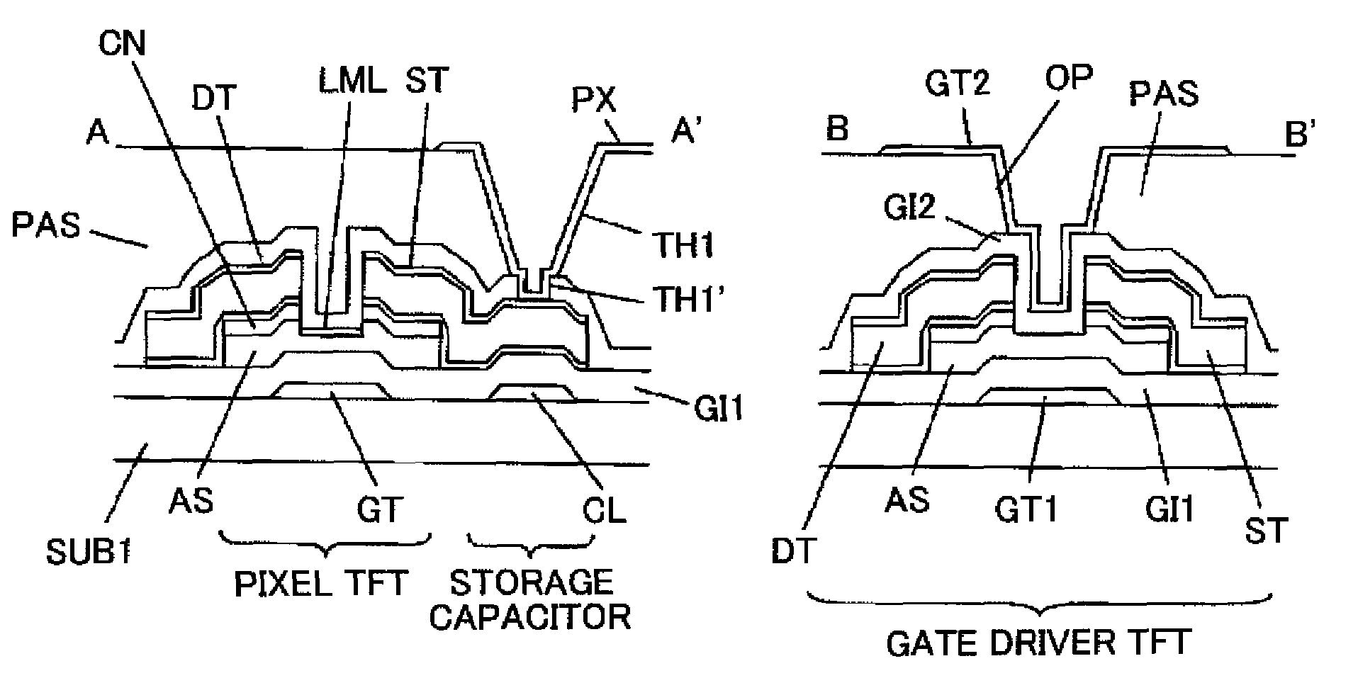
[0071]FIG. 12 is a cross-sectional view illustrating a pixel TFT and a gate driver TFT according to the present invention, and is drawn in a corresponding manner to FIG. 1. The pixel TFT has, as in FIG. 1, the low mobility layer LML formed on the front side of the semiconductor film AS. The semiconductor film AS is formed thinner in regions that are not covered with the source ST and drain DT of the gate driver TFT than in regions that are not covered with the source ST and drain ST of the pixel TFT, and a part of the semiconductor film AS of the gate driver TFT including the low mobility layer that is formed temporarily in the process of this embodiment is removed. Also in this embodiment, the mobility on the front side of the semiconductor film AS of the gate driver TFT is higher than the mobility on the front side of the semiconductor film AS of the pixel TFT, and the gate driver TFT which is a dual gate TFT having a large driving power and the pixel TFT that is reduced in leakag...

third embodiment

[0074]FIGS. 15 and 16 are diagrams illustrating a method of manufacturing a pixel TFT and a gate driver TFT according to the present invention, and each illustrate one of manufacturing steps for the pixel TFT and the gate driver TFT.

[0075]After the structure described above with reference to FIG. 7 is formed, the three-layer metal film MT made up of a Mo alloy layer and Al alloy layers is formed by deposition through sputtering as in the above description. As illustrated in FIG. 15, photoresist RST1 is formed for processing with which the source ST and drain DT of the pixel TFT are formed while a region that is to become the gate driver TFT is covered. The metal film MT is etched in this state. The exposed part of the contact layer CN and part of the semiconductor film AS are also etched, and then plasma treatment is performed to form the low mobility layer LML on the front side of the semiconductor film AS of the pixel TFT. Next, as illustrated in FIG. 16, the photoresist RST1 is r...

fourth embodiment

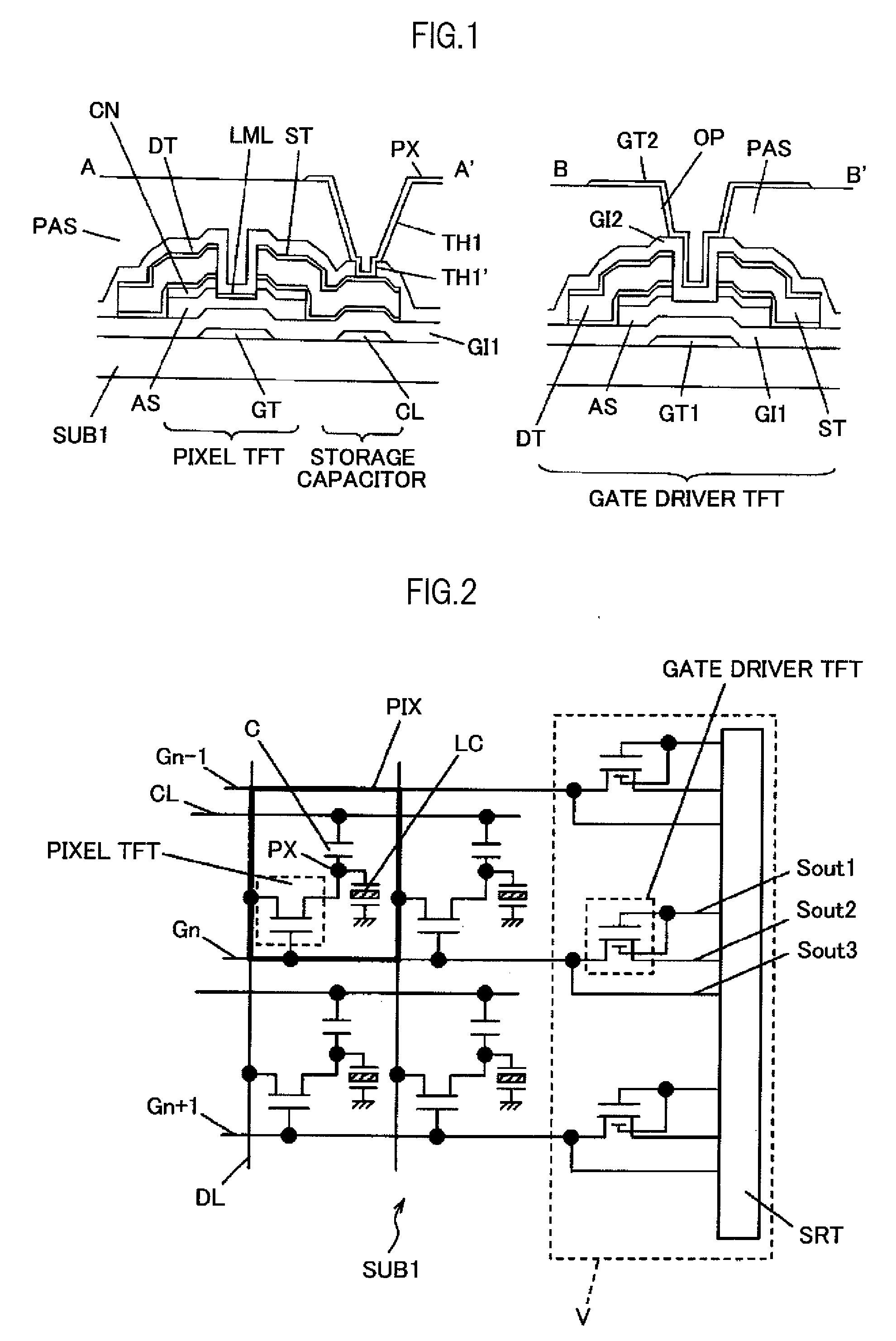
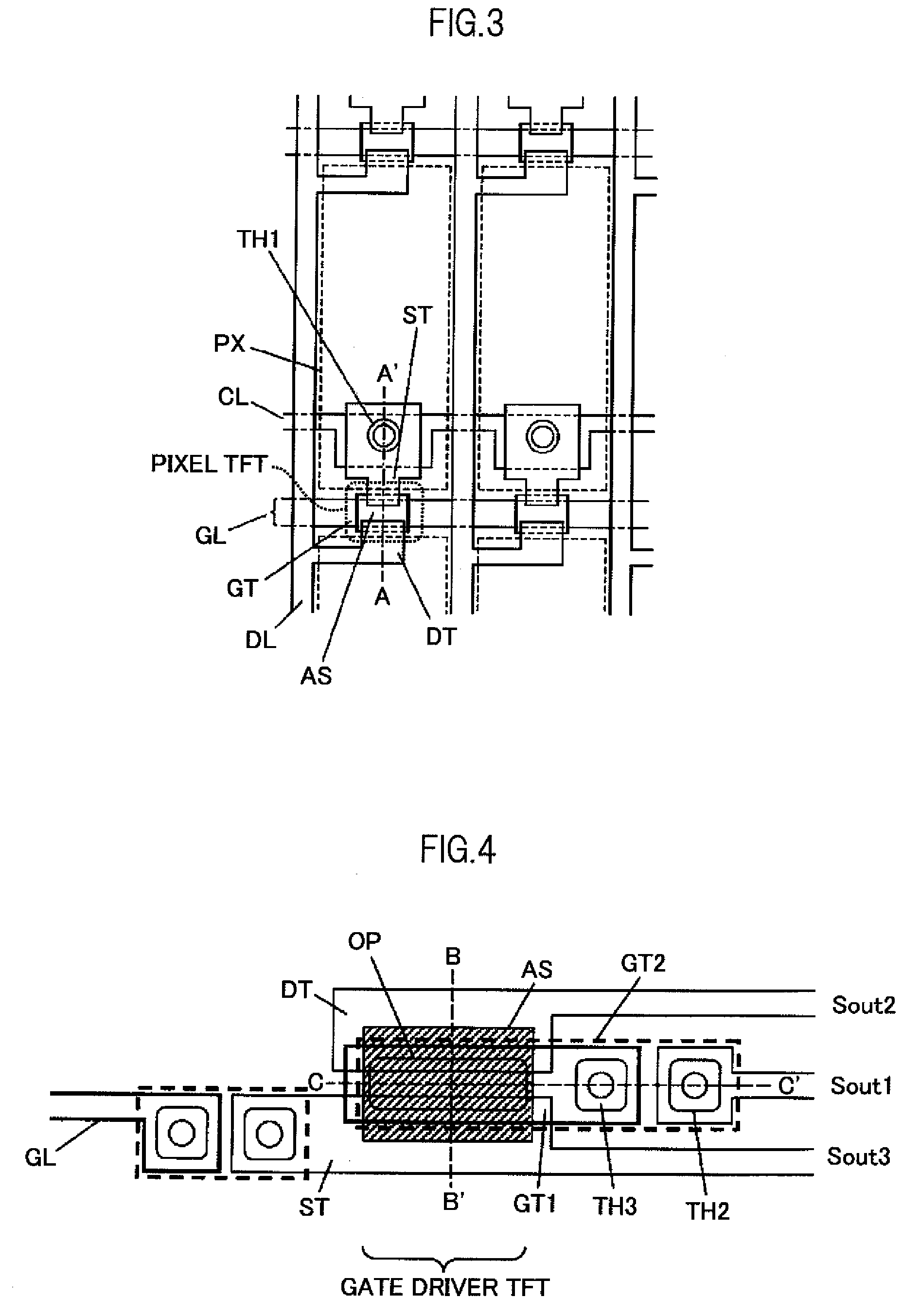
[0077]FIG. 17 illustrates an example of an equivalent circuit of a horizontal electric field type (in-plane-switching type) liquid crystal display device according to the present invention, and is drawn in a corresponding manner to FIG. 2. As in FIG. 2, a pixel and the gate driver circuit V which are formed of TFTs are formed on the same substrate SUB1. In the horizontal electric field type liquid crystal display device, the pixel electrode PX and a counter electrode CT are both formed on the TFT substrate SUB1 side. A voltage applied to the counter electrode CT through a counter voltage line CTL serves as a reference for a voltage applied to the pixel electrode PX. A storage capacitor is formed between the pixel electrode PX and the counter electrode CT. A pixel TFT is formed in the pixel PIX. The low mobility layer LML is formed on the front side of the semiconductor film AS of the pixel TFT. A gate driver TFT of dual gate type is formed in the gate driver circuit V to control the...


PUM


Abstract

Provided is an image display device comprising, on a TFT substrate: a plurality of gate lines and a plurality of drain lines which intersect with each other; a pixel TFT provided within a pixel which is enclosed by a pair of adjacent gate lines and a pair of adjacent drain lines; a gate driver TFT which is connected to one of the plurality of gate lines to drive the one of the plurality of gate lines, wherein the pixel TFT and the gate driver TFT each include an amorphous semiconductor film as a channel, wherein the pixel TFT has a bottom gate structure, wherein the gate driver TFT has a dual gate structure, and wherein a mobility on a top surface side of the semiconductor film of the gate driver TFT is higher than a mobility on a top surface side of the semiconductor film of the pixel TFT.

Description

CROSS-REFERENCE TO RELATED APPLICATION[0001]The present application claims priority from Japanese application JP 2008-187246 filed on Jul. 18, 2008, the content of which is hereby incorporated by reference into this application.BACKGROUND OF THE INVENTION[0002]1. Field of the Invention[0003]The present invention relates to an image display device and a manufacturing method therefor. More particularly, the present invention relates to an image display device with a built-in driver circuit which includes a driver circuit on a substrate, and a method of manufacturing the image display device.[0004]2. Description of the Related Art[0005]There has been known a type of liquid crystal display device which uses a thin film transistor (hereinafter may simply be referred to as TFT) with a semiconductor film made of amorphous silicon, especially a bottom gate TFT which includes a gate electrode provided on a substrate side with respect to the semiconductor film (underside of the semiconductor ...

Claims


Application Information

Patent Timeline
IPC IPC(8): H01L33/00H01L29/786H01L21/336
CPCH01L27/1214H01L29/78648H01L27/1251H01L27/1233
Inventor SATO, TAKESHI
Owner PANASONIC LIQUID CRYSTAL DISPLAY CO LTD
Why Eureka
Try Eureka