A kind of carrying device and method for rapid splitting of pss substrate wafer

A technology for carrying devices and wafers, which is applied to semiconductor devices, electrical components, circuits, etc., can solve problems such as unseen related reports, and achieve the effects of easy control and operation and simple device structure.

Active Publication Date: 2018-11-09
浙江美宝物联网科技股份有限公司
View PDF4 Cites 0 Cited by
  • Summary
  • Abstract
  • Description
  • Claims
  • Application Information

AI Technical Summary

Problems solved by technology

Before SEM analysis, the sample should be prepared first, and the back of the PSS substrate to be tested should be divided into several blocks with a diamond pen, and then split, that is, several blocks that have been drawn by the diamond pen will be split. What kind of device and method has not been seen in the prior art, and how to split the sample quickly and conveniently is the key problem to be solved by the present invention

Method used


Image

  • A kind of carrying device and method for rapid splitting of pss substrate wafer
  • A kind of carrying device and method for rapid splitting of pss substrate wafer

Examples


Embodiment 1

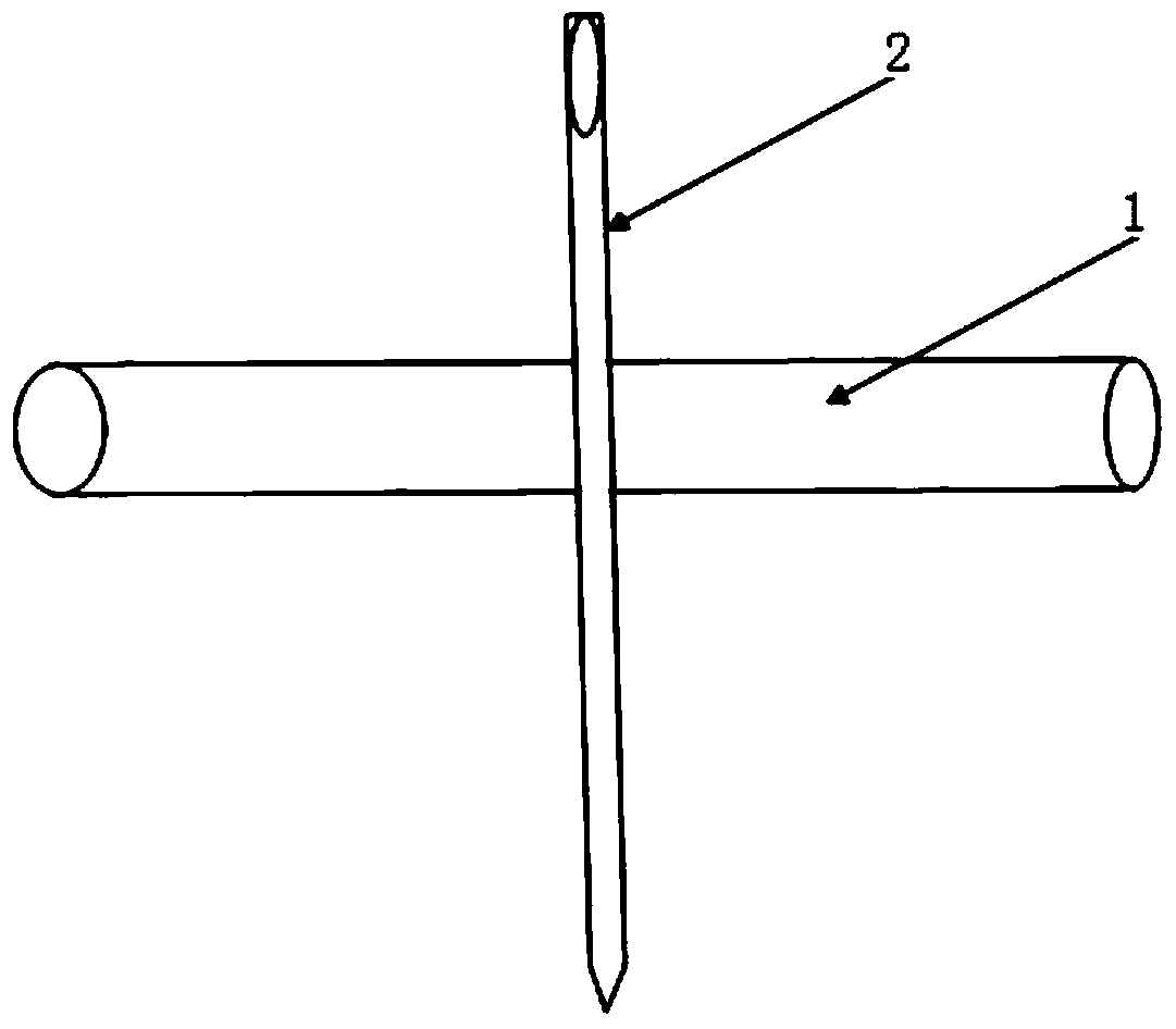
[0027] The carrying device of the present invention is made by taking a plastic rod 1 with a diameter of 5 mm and a length of 50-100 mm; taking a sewing needle 2 with a length of 50-80 mm; using the needle point of the sewing needle in the middle of the plastic rod 1 and insert the sewing needle 2 into the plastic rod 1, which can move up and down as required. The present invention is used as the carrying device of the PSS substrate wafer 3. During the split sample preparation process, a diamond knife is used Draw a knife scratch 4 along the line to be cracked on the back of the wafer, and then place the wafer to be cracked face up on the carrier, so that the diamond knife scratch and the sewing needle are in the same longitudinal and vertical direction. Mouth, press firmly with tweezers figure 2 The force point A of the lobes in the chip can split the wafer along the scratch of the diamond knife, which is convenient and fast.


PUM


Abstract

The invention discloses a bearing device and method for rapid division of a patterned sapphire substrate (PPS) chip. The bearing device comprises a bearing rack, wherein the bearing rack is used for placing the PSS chip and comprises a transverse rod and a longitudinal rod, the transverse rod and the longitudinal rod are connected in a staggered manner, and the transverse rod is arranged at the rear end position of the middle part of the longitudinal rod. By the bearing device, the defect of the prior art is overcome, the substrate to be divided can be placed on the bearing device disclosed by the invention during PSS analysis and sampling, so that the substrate can be rapidly and conveniently divided to complete sample preparation.

Description

technical field [0001] The invention relates to the technical field of LED chips, in particular to a carrying device and method for rapid splitting of PSS substrate wafers. Background technique [0002] In order to improve the brightness of LED chips, it is necessary to conduct research and development on the PSS (patterned sapphire substrate) substrate (two inches or four inches, the same below) used for growing epitaxial wafers. The three-dimensional shape of the graph (height, bottom width and period, etc.). Before SEM analysis, the sample should be prepared first, and the back of the PSS substrate to be tested should be divided into several blocks with a diamond pen, and then split, that is, several blocks that have been drawn by the diamond pen will be split. What kind of device and method has not been seen in the prior art, and how to split the sample quickly and conveniently is the key problem to be solved by the present invention. Contents of the invention [000...

Claims


Application Information

Patent Timeline
Patent Type & Authority Patents(China)
IPC IPC(8): H01L21/687H01L33/00
CPCH01L21/68785H01L33/00H01L33/005
Inventor 王永妍
Owner 浙江美宝物联网科技股份有限公司
Why Eureka
Try Eureka