A high-performance magnetoresistive device and its manufacturing process

A magnetoresistive device, high-performance technology, applied in the fields of magnetic field-controlled resistors, the manufacture/processing of electromagnetic devices, semiconductor devices, etc., can solve the problems of small input resistance and cannot be practically applied, and achieve the effect of large input impedance

Active Publication Date: 2019-02-12
浙江森尼克半导体有限公司
View PDF3 Cites 0 Cited by
  • Summary
  • Abstract
  • Description
  • Claims
  • Application Information

AI Technical Summary

Problems solved by technology

However, due to the small input resistance, it cannot be practically applied

Method used


Image

  • A high-performance magnetoresistive device and its manufacturing process
  • A high-performance magnetoresistive device and its manufacturing process
  • A high-performance magnetoresistive device and its manufacturing process

Examples


Embodiment 1

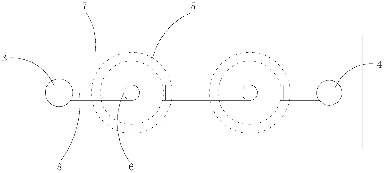
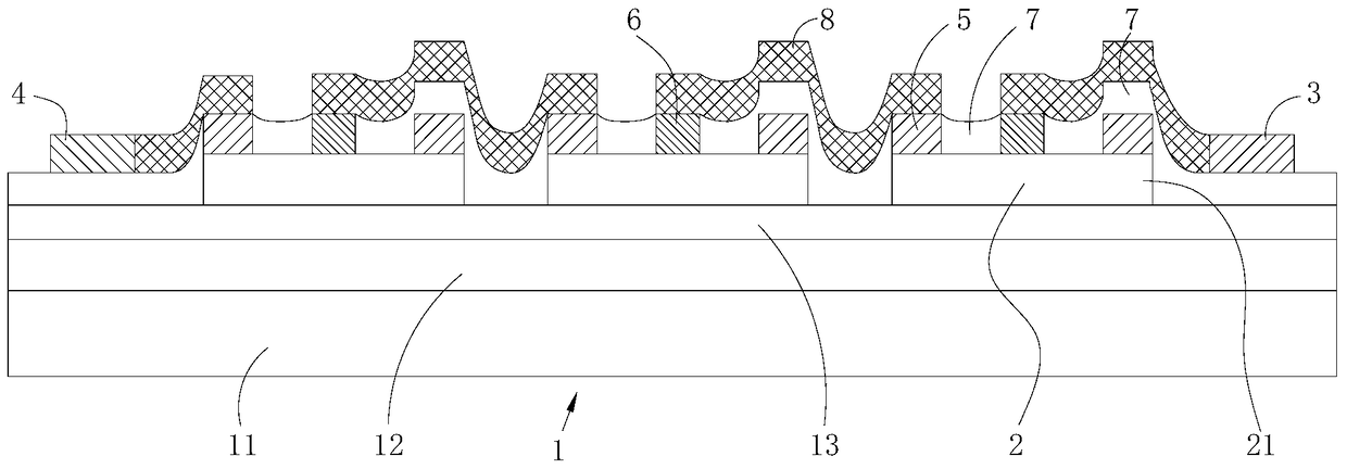
[0034] Refer to attached figure 2 (refer to attached image 3 ), a high-performance magnetoresistive device in this embodiment, which includes a substrate 1 (attached figure 2 covered under the insulating film), a plurality of InSb thin film disks 2 arranged in sequence on the substrate 1 (attached figure 2 covered under the insulating film), the ring electrode 5 on the InSb thin film disk 2 (attached figure 2 In the figure, the part where the ring electrode is covered under the insulating film is indicated by a dotted line), the center electrode 6 on the InSb thin film disk 2 and inside the ring electrode 5 (attached figure 2 Covered by the connecting electrode 8 ), on the ring electrode 5 and partly covering the insulating film 7 of the ring electrode 5 .

[0035] The insulating film 7 covers each ring electrode 5, and a plurality of first openings and a plurality of second openings are opened above each ring electrode 5 so that each ring electrode 5 has a part from ...

Embodiment 2

[0047] Refer to attached image 3 , the difference between a high-performance magnetoresistive device in this embodiment and the first embodiment is only that: the number of InSb thin film disks 2 and connecting electrodes 8 is different from that of the first embodiment.

[0048] In this embodiment, the first electrode 3 is a negative electrode, and the second electrode 4 is a positive electrode.

[0049] The substrate 1 in this embodiment includes a substrate layer 11 , a transition layer 12 , and an insulating layer 13 arranged in sequence from bottom to top. The thickness of the substrate layer 11 is 100 μm-1000 μm, and the material is ceramic, silicon, ferrite or mica. The thickness of the insulating layer 13 is 0.01 μm to 10 μm, and the material is In 2 o 3 or SiO 2. The material of the transition layer 12 is a compound containing at least one metal element in the same group as In including In. The compound contains at least Sb, and the compound only contains metal ...


PUM


Abstract

The invention discloses a high-performance magnetoresistive device and its manufacturing process. Through the serial structure of a plurality of Cobino disks, the traditional strip-shaped magnetoresistive device is replaced, and while obtaining the maximum magnetoresistance effect, it also has larger input resistance.

Description

technical field [0001] The invention relates to a high-performance magnetoresistive device and a manufacturing process. Background technique [0002] In the strip-shaped magnetoresistive device in the prior art, due to the Hall effect, positive and negative charges will accumulate on both sides of the magnetoresistive device respectively, so multiple magnetoresistive devices will be set on the magnetoresistive device extending from one side to the other. The short-circuit bar 9 to eliminate the accumulated charge, as attached figure 1 , however, this method cannot completely eliminate the accumulated charges, and there will still be residual charges between the short-circuit bars, so the effect is limited. Physically, the Corbino disk has the highest magnetoresistance effect. However, due to the small input resistance, it cannot be practically applied. Contents of the invention [0003] In order to overcome the above disadvantages, the object of the present invention is...

Claims


Application Information

Patent Timeline
Patent Type & Authority Patents(China)
IPC IPC(8): H01L27/22H01L43/08H01L43/02H01L43/12
CPCH10B61/00H10N59/00H10N50/80H10N50/01H10N50/10
Inventor 马可军俞振中郑律
Owner 浙江森尼克半导体有限公司
Why Eureka
Try Eureka