Crystal bar cutting method and wire saw
A technology of ingots and steel wires, applied in the field of cutting methods and wire saws, can solve problems such as thinning, and achieve the effect of improving productivity and consistent processing conditions
- Summary
- Abstract
- Description
- Claims
- Application Information
AI Technical Summary
Problems solved by technology
Method used
Image
Examples
Embodiment 1
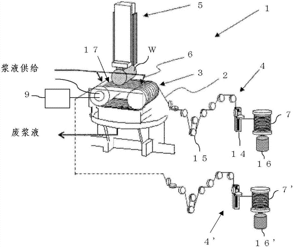
[0057] Such as figure 1 As shown, in the wire saw of the present invention, after replacing the steel wire with a steel wire in a new state, the cutting method of the present invention repeatedly performs cutting of a plurality of ingots.
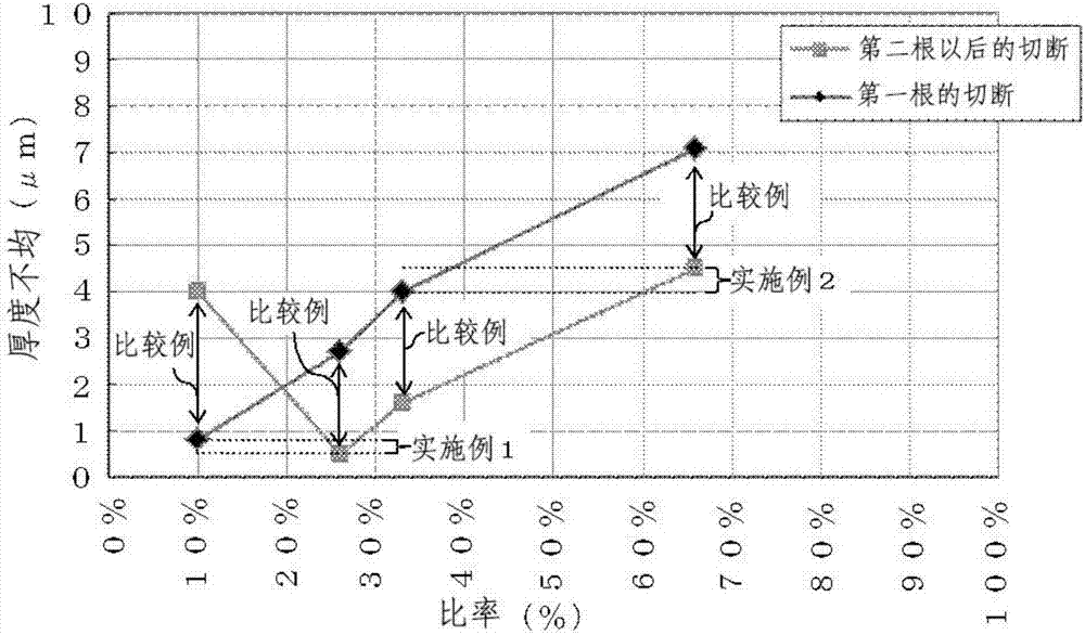
[0058] The thickness unevenness of each wafer cut from each ingot was measured, and the average value of the thickness unevenness of each wafer cut from each ingot was calculated. In addition, the term “uneven thickness” refers to the difference between the thickness of the cutting start portion and the thickness of the center portion in the wafer surface as described above.
[0059] In Example 1, when the first ingot was cut after replacing the steel wire, when cutting the central part of the ingot, the new steel wire per unit time when cutting the cutting start part of the ingot was supplied. The ratio of the amount is set to 10%. Then, when cutting the second and subsequent ingots, the ratio of the new wire supply amount per unit time at th...
Embodiment 2
[0062] Except that the above ratio was set to 33% when the first ingot was cut after replacing the steel wire, and the above ratio was set to 66% when the second and subsequent ingots were cut, the same as in Example 1 was used. Condition, repeated cutting of the ingot. That is, the above-mentioned ratio when the first ingot is cut is 1 / 2 of the above-mentioned ratio when the second and subsequent ingots are cut.
[0063] After the cutting of the ingot was completed, the thickness unevenness was measured by the same method as in Example 1, and the average value was calculated.
[0064] The result is image 3 As shown in Table 1, the average thickness of the wafer cut from the first ingot is 4.0 μm. In addition, the average thickness of the wafers cut from the second and subsequent ingots was 4.5 μm. Therefore, the difference in thickness unevenness was 0.5 μm, and as in Example 1, it was confirmed that the unevenness in thickness became very small.
PUM
 Abstract
Description
Claims
Application Information


