Array substrate, display and electronic equipment

An array substrate and electrical connection technology, applied in the field of touch display, can solve problems such as affecting the accuracy of touch detection, and achieve the effects of avoiding parasitic capacitance, increasing the aperture ratio, and reducing the width of shading areas

Active Publication Date: 2016-04-20
SHANGHAI TIANMA MICRO ELECTRONICS CO LTD +1
View PDF3 Cites 9 Cited by
  • Summary
  • Abstract
  • Description
  • Claims
  • Application Information

AI Technical Summary

Problems solved by technology

[0004] In the above-mentioned touch display panel, the common wiring 14 will form a parasitic capacitance with the opposite data line 16, which will af

Method used


Image

  • Array substrate, display and electronic equipment
  • Array substrate, display and electronic equipment
  • Array substrate, display and electronic equipment

Examples


Embodiment Construction

[0027] The following will clearly and completely describe the technical solutions in the embodiments of the present invention with reference to the accompanying drawings in the embodiments of the present invention. Obviously, the described embodiments are only some, not all, embodiments of the present invention. Based on the embodiments of the present invention, all other embodiments obtained by persons of ordinary skill in the art without making creative efforts belong to the protection scope of the present invention.

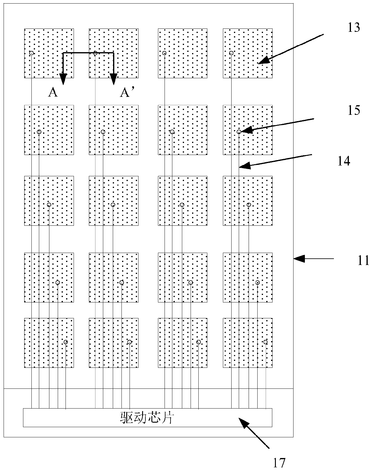
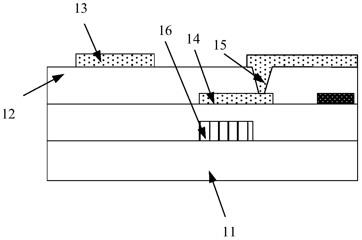
[0028] As in the background technology, figure 1 and figure 2 In the touch display panel of the prior art shown, the common wiring 14 will form a parasitic capacitance with the opposite data line 16, which will affect the accuracy of touch detection during touch detection, especially in the application of medium and large size panels. , the problem is obvious.

[0029] In order to solve the above problems, an embodiment of the present invention provides an ...


PUM


Abstract

The invention discloses an array substrate, a display and electronic equipment. The array substrate comprises a public electrode layer and a pixel electrode layer which are opposite to each other, wherein the pixel electrode layer comprises a plurality of arrayed pixel electrodes, and the public electrode layer comprises a plurality of public electrode blocks; the array substrate further comprises a plurality of switch devices, a plurality of data lines extending along the column direction of the array, and a plurality of public routings electrically connected with the public electrode blocks in a one-to-one correspondence manner; projections of the public routings in the pixel electrode layer are not superposed with the pixel electrodes in the direction vertical to the pixel electrode layer; a pixel clearance is reserved between every two adjacent pixel electrodes; projections of the public routings in the pixel electrode layer and projections of the data lines in the pixel electrode layer are positioned in different pixel clearances in the direction vertical to the pixel electrode layer; two data lines of which the projections are positioned in the same pixel clearance are positioned on different layers. The array substrate is higher in touch detection precision.

Description

technical field [0001] The present invention relates to the technical field of touch display, and more specifically, to an array substrate, a display and an electronic device. Background technique [0002] With the development of science and technology, more and more touch display devices are used in people's daily life and work, bringing great convenience to people's daily life and work, and becoming an indispensable tool for people today. . The main component of a touch display device is a touch display panel. [0003] refer to figure 1 and figure 2 , figure 1 It is a top view of a common touch display panel in the prior art, figure 2 for figure 1 The sectional view of the touch display panel in the AA' direction is shown, and the touch display panel includes: a substrate 11; a common electrode layer and a common wiring layer arranged on the surface of the substrate 11. Wherein, the common electrode layer and the common wiring layer are located in different conduc...

Claims


Application Information

Patent Timeline
IPC IPC(8): G06F3/041
CPCG06F3/041G06F3/0412G02F1/13338G09G3/32G09G2300/0426G09G2310/0278G09G2320/0219G02F1/136286G06F3/0443H10K59/131
Inventor 周星耀姚绮君卢峰杨康
Owner SHANGHAI TIANMA MICRO ELECTRONICS CO LTD
Why Eureka
Try Eureka