Optical Image Capturing System

An optical imaging system and imaging surface technology, applied in optics, optical components, instruments, etc., can solve problems such as inability to meet photography requirements

Inactive Publication Date: 2016-05-18
ABILITY OPTO ELECTRONICS TECH
View PDF5 Cites 10 Cited by
  • Summary
  • Abstract
  • Description
  • Claims
  • Application Information

AI Technical Summary

Problems solved by technology

[0004] Traditional optical systems mounted on portable devices mostly use four-element or five-element lens structures. However, due to the continuous improvement of pixels in portable devices and the demand for large apertures such as low-light and night shooting functions from end consumers, existing The advanced optical imaging system can no longer meet the higher-level photography requirements

Method used


Image

  • Optical Image Capturing System
  • Optical Image Capturing System
  • Optical Image Capturing System

Examples


no. 1 example

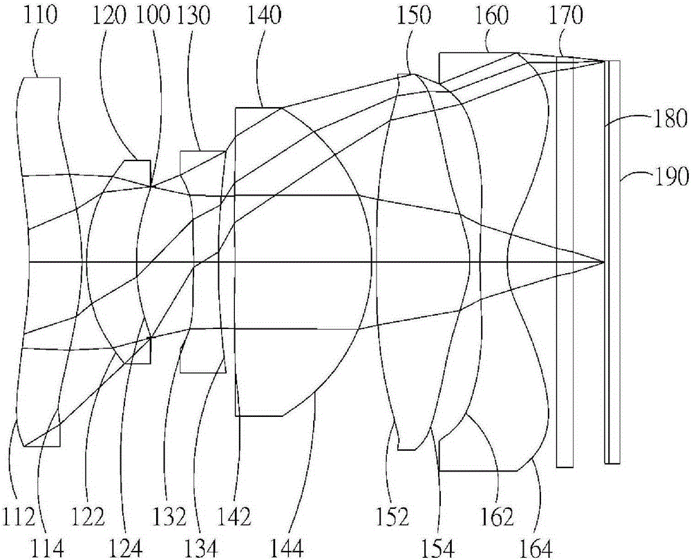
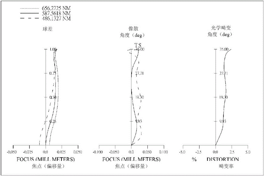
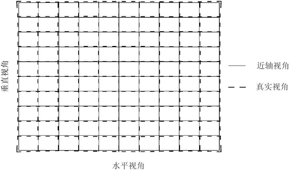
[0185] Please refer to Figure 1A and Figure 1B ,in Figure 1A Representing a schematic diagram of an optical imaging system according to a first embodiment of the present invention, Figure 1B From left to right are the spherical aberration, astigmatism and optical distortion curves of the optical imaging system of the first embodiment. Figure 1C It is a TV distortion curve diagram of the optical imaging system of the first embodiment. Depend on Figure 1A It can be seen that the optical imaging system includes a first lens 110, an aperture 100, a second lens 120, a third lens 130, a fourth lens 140, a fifth lens 150, a sixth lens 160, and an infrared filter from the object side to the image side. 170 , an imaging surface 180 and an image sensing element 190 .

[0186] The first lens 110 has positive refractive power and is made of plastic material. The object side 112 is concave, and the image side 114 is convex, both of which are aspherical. The object side 112 has an i...

no. 2 example

[0228] Please refer to Figure 2A and Figure 2B ,in Figure 2A A schematic diagram showing an optical imaging system according to a second embodiment of the present invention, Figure 2B From left to right are the spherical aberration, astigmatism and optical distortion curves of the optical imaging system of the second embodiment. Figure 2C It is a TV distortion curve diagram of the optical imaging system of the second embodiment. Depend on Figure 2A It can be seen that the optical imaging system sequentially includes an aperture 200, a first lens 210, a second lens 220, a third lens 230, a fourth lens 240, a fifth lens 250, a sixth lens 260, and an infrared filter from the object side to the image side. 270 , an imaging surface 280 and an image sensing element 290 .

[0229] The first lens 210 has positive refractive power and is made of plastic material. The object side 212 is convex, and the image side 214 is convex, both of which are aspherical. The object side 21...

no. 3 example

[0255] Please refer to Figure 3A and Figure 3B ,in Figure 3A A schematic diagram showing an optical imaging system according to a third embodiment of the present invention, Figure 3B From left to right are the spherical aberration, astigmatism and optical distortion curves of the optical imaging system of the third embodiment. Figure 3C is a TV distortion curve diagram of the optical imaging system of the third embodiment. Depend on Figure 3A It can be seen that the optical imaging system includes an aperture 300, a first lens 310, a second lens 320, a third lens 330, a fourth lens 340, a fifth lens 350, a sixth lens 360, and an infrared filter from the object side to the image side. 370 , an imaging surface 380 and an image sensing element 390 .

[0256]The first lens 310 has positive refractive power and is made of plastic material. The object side 312 is convex, and the image side 314 is convex, both of which are aspherical. The image side 314 has an inflection p...


PUM


Abstract

An optical image capturing system, from an object side to an image side, comprises a first, second, third, fourth, fifth and sixth lens elements. The first through fifth lens elements have refractive power and both of an object-side surface and an image-side surface of the fifth lens elements are aspheric. The sixth lens with negative refractive power may have a concave image-side surface. Both of the image-side surface and the object-side surface of the six lens elements are aspheric and at least one of the two surfaces has inflection points. Each of the six lens elements may have refractive power. When specific conditions are satisfied, the optical image capturing system can have a large aperture value and a better optical path adjusting ability to acquire better imaging quality.

Description

technical field [0001] The invention relates to an optical imaging system, and in particular to a miniaturized optical imaging system applied to electronic products. Background technique [0002] In recent years, with the rise of portable electronic products with photography functions, the demand for optical systems has increased day by day. The photosensitive element of the general optical system is nothing more than a photosensitive coupling element (Charge Coupled Device; CCD) or a complementary metal oxide semiconductor element (Complementary [0003] Metal-OxideSemiconductorSensor; CMOSSensor) two types, and with the improvement of semiconductor manufacturing process technology, the pixel size of the photosensitive element is reduced, and the optical system is gradually developing into the high-pixel field, so the requirements for imaging quality are also increasing. [0004] Traditional optical systems mounted on portable devices mostly use four-element or five-elemen...

Claims


Application Information

Patent Timeline
Patent Type & Authority Applications(China)
IPC IPC(8): G02B13/18G02B13/00
CPCG02B13/0045
Inventor 唐乃元张永明
Owner ABILITY OPTO ELECTRONICS TECH
Why Eureka
Try Eureka