Method and apparatus for patterned wafer characterization
A wafer and characterization technology, used in instruments, measuring devices, scientific instruments, etc., can solve the problems of time-consuming, failure to provide subsurface defect structures, etc.
- Summary
- Abstract
- Description
- Claims
- Application Information
AI Technical Summary
Problems solved by technology
Method used
Image

Examples
Embodiment Construction
[0028] In the following description, numerous specific details are set forth in order to provide a thorough understanding of the present invention. The present invention may be practiced without some or all of these specific details. In other instances, well known process operations have not been described in detail so as not to unnecessarily obscure the present invention. While the invention will be described in conjunction with specific embodiments, it will be understood that it is not intended to limit the invention to the described embodiments.
[0029] Introduction
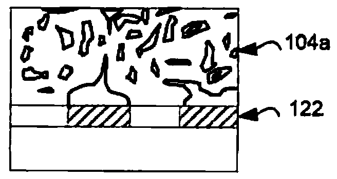
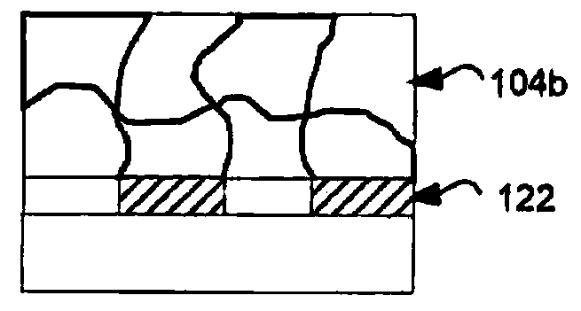
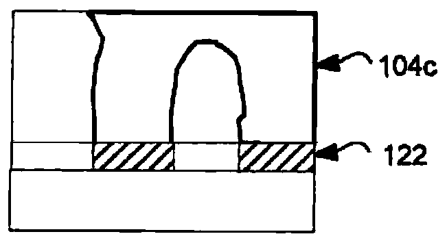
[0030] Directed self-assembly (DSA) is currently being explored by many groups as a patterning technique for advanced nodes. Figures 1A to 1D To illustrate the DSA process utilizing the guiding pattern 122, the block copolymer material becomes more and more self-ordered onto the guiding pattern 122 during the annealing process. As shown, the block copolymer material 104a is initially relative to Figure ...
PUM
 Abstract
Description
Claims
Application Information
 - R&D
- Intellectual Property
- Life Sciences
- Materials
- Tech Scout
- Unparalleled Data Quality
- Higher Quality Content
- 60% Fewer Hallucinations
Browse by: Latest US Patents, China's latest patents, Technical Efficacy Thesaurus, Application Domain, Technology Topic, Popular Technical Reports.
© 2025 PatSnap. All rights reserved.Legal|Privacy policy|Modern Slavery Act Transparency Statement|Sitemap|About US| Contact US: help@patsnap.com