Printed circuit boards, camera modules and mobile terminals

A technology of printed circuit boards and camera modules, which is applied in the direction of printed circuits, printed circuits, printed circuit components, etc., can solve the problems of increasing inventory risks, increasing production costs and production cycles, waste of manpower and material resources, etc., to reduce inventory risks , Control production cost and the effect of production cycle

Active Publication Date: 2018-09-04
GUANGDONG OPPO MOBILE TELECOMM CORP LTD
View PDF4 Cites 0 Cited by
  • Summary
  • Abstract
  • Description
  • Claims
  • Application Information

AI Technical Summary

Problems solved by technology

[0003] However, for camera modules with different pixels, although they have the same component packaging structure, the signal sequence of the component pins is not exactly the same, so that in the manufacturing process of different pixel products, they need to be designed separately. Printed Circuit Board (PCB), and use different product lines to achieve component placement and debugging
Therefore, since PCBs cannot be shared between products with different pixels, it will undoubtedly increase the production cost and production cycle of the product, resulting in unnecessary waste of manpower and material resources; at the same time, different product models use different PCBs, which will also increase inventory risks.

Method used


Image

  • Printed circuit boards, camera modules and mobile terminals
  • Printed circuit boards, camera modules and mobile terminals
  • Printed circuit boards, camera modules and mobile terminals

Examples


Embodiment Construction

[0023] The following will clearly and completely describe the technical solutions in the embodiments of the present invention with reference to the accompanying drawings in the embodiments of the present invention. Obviously, the described embodiments are only some, not all, embodiments of the present invention. Based on the embodiments of the present invention, all other embodiments obtained by persons of ordinary skill in the art without making creative efforts belong to the protection scope of the present invention.

[0024] For ease of description, spatially relative terms such as "under", "beneath", "below", "above", "on" and other spatially relative terms may be used herein to describe an element as shown in the drawings Or the relationship of a feature to another element or feature(s). It will be understood that when an element or layer is referred to as being "on," "connected to," or "coupled to" another element or layer, it can be directly on, directly on, or directly...


PUM


Abstract

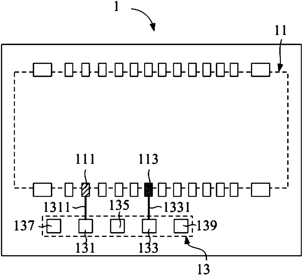
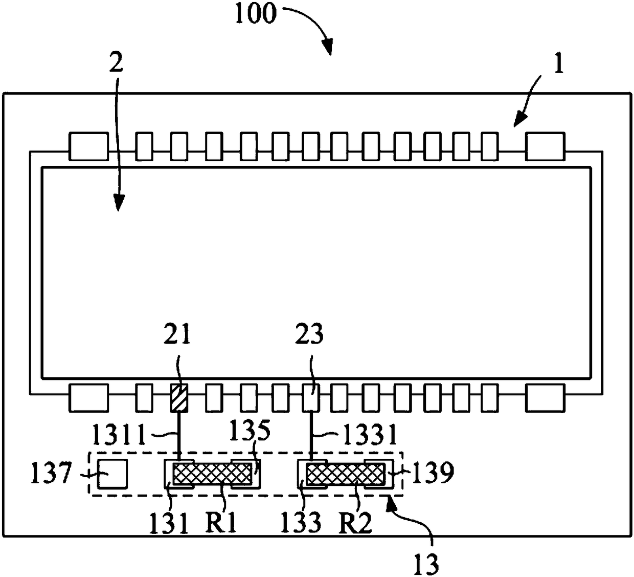
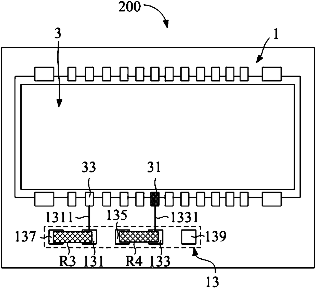
The invention provides a printed circuit board. The printed circuit board comprises a first bonding pad set and a second bonding pad set, wherein the first bonding pad set comprises a first functional bonding pad and a second functional bonding pad, the second bonding pad set comprises a first bonding pad, a second bonding pad and a third bonding pad, the first bonding pad is connected with the first functional bonding pad through first routing, the second bonding pad is connected with the second functional bonding pad through second routing, the third bonding pad is arranged between the first bonding pad and the second bonding pad, and the third bonding pad is connected with a first signal path; the first bonding pad and the third bonding pad are connected through a first resistor; and the second bonding pad and the third bonding pad are connected through a fourth resistor. Moreover, the invention also provides a shooting module using the printed circuit board and a mobile terminal using the shooting module. The printed circuit board can realize PCB sharing among shooting modules with different pixels.

Description

technical field [0001] The invention relates to the field of electronic technology, in particular to a printed circuit board, a camera module and a mobile terminal. Background technique [0002] At present, high-definition camera modules have been more and more widely used in mobile terminals such as smart phones and tablet computers. With the improvement of the imaging quality of the built-in camera module of the mobile terminal, people no longer need to carry a relatively bulky digital camera in daily travel, but can directly use the camera module built in the mobile terminal to complete high-quality image shooting. In order to enrich the product models of mobile terminals, a popular mobile terminal product may include many different models, and the price ranges of each model of mobile terminals are different, so as to meet the needs of different consumer groups. Usually, in order to control the production cost of different models of products and reflect the performance d...

Claims


Application Information

Patent Timeline
Patent Type & Authority Patents(China)
IPC IPC(8): H05K1/11H05K1/18
CPCH05K1/11H05K1/181H05K2201/09418
Inventor 曾元清
Owner GUANGDONG OPPO MOBILE TELECOMM CORP LTD
Why Eureka
Try Eureka