Manufacturing method of film transistor structure

A technology of thin film transistors and manufacturing methods, which is applied in the field of manufacturing thin film transistor structures, can solve problems such as high complexity, and achieve the effect of simplifying the manufacturing process

Inactive Publication Date: 2016-06-08
TCL CHINA STAR OPTOELECTRONICS TECH CO LTD
View PDF3 Cites 4 Cited by
  • Summary
  • Abstract
  • Description
  • Claims
  • Application Information

AI Technical Summary

Problems solved by technology

[0004] In view of this, the present invention provides a method for manufacturing a thin film transistor structure to solve the high complexity of the manufacturing process in the prior art and the problems caused by the use of an etch barrier layer

Method used


Image

  • Manufacturing method of film transistor structure
  • Manufacturing method of film transistor structure
  • Manufacturing method of film transistor structure

Examples


Embodiment Construction

[0020] The following descriptions of the various embodiments refer to the accompanying drawings to illustrate specific embodiments in which the present invention can be practiced. Furthermore, the directional terms mentioned in the present invention are, for example, up, down, top, bottom, front, back, left, right, inside, outside, side, surrounding, central, horizontal, transverse, vertical, longitudinal, axial, The radial direction, the uppermost layer or the lowermost layer, etc. are only directions referring to the attached drawings. Therefore, the directional terms used are used to illustrate and understand the present invention, but not to limit the present invention.

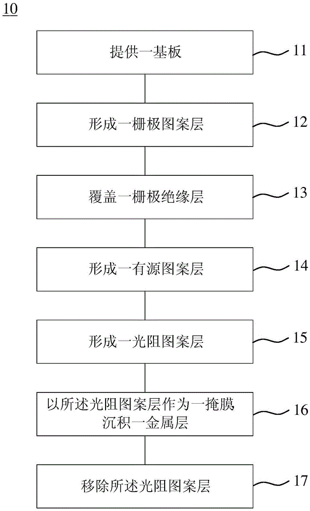
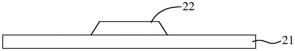
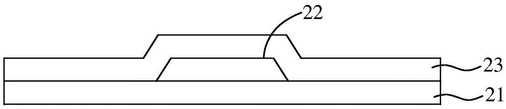
[0021] Please refer to figure 1 as shown, figure 1 It is a flow chart illustrating a manufacturing method 10 of a thin film transistor structure according to an embodiment of the present invention. A manufacturing method 10 of a thin film transistor structure according to an embodiment of the present i...


PUM

PropertyMeasurementUnit
angleaaaaaaaaaa

Abstract

The invention discloses a manufacturing method of a film transistor structure. A photoresistive pattern layer is formed on an active pattern layer and a part of grid electrode insulating layer so as to expose a source electrode predetermined position and a drain electrode predetermined position of the grid electrode insulating layer. The photoresistive pattern layer comprises a plurality of inverted-trapezoid blocks and can also be used as a mask so as to deposit a metal layer on the photoresistive pattern layer, the source electrode predetermined position and the drain electrode predetermined position. After the photoresistive pattern layer and the metal layer thereon are removed, the residual metal layer patterns are converted into a source electrode and a drain electrode. According to the invention, the manufacturing process is simplified, and an etching barrier layer for protecting back channels is not formed.

Description

technical field [0001] The invention relates to a manufacturing method of a semiconductor structure, in particular to a manufacturing method of a thin film transistor structure. Background technique [0002] In the manufacturing process of traditional oxide semiconductor thin film transistors, such as Indium Gallium Zinc Oxide Thin Film Transistor (IGZOTFT), in order to protect the back channel from etching damage during the etching process of the source and drain An etching stopper (ESL) is formed on the semiconductor layer, thereby adding a mask procedure and increasing the complexity of the manufacturing process of the thin film transistor. In addition, the etch stop layer, besides limiting the length of the channel, is difficult to implement in display devices with higher resolution. Furthermore, in the manufacturing process of the traditional thin film transistor, in order to form the source and the drain, a mask procedure is required, which increases the complexity of...

Claims


Application Information

Patent Timeline
Patent Type & Authority Applications(China)
IPC IPC(8): H01L21/34H01L21/027
CPCH01L21/0274H01L29/66969H01L21/027H01L21/34C23C14/185H01L27/1288H01L29/4908H01L29/41733H01L29/7869H10K71/233H10K71/621H10K71/221C23C14/34H01L21/0272H01L21/28506H01L21/443H01L27/1225H01L27/127H01L29/78696H01L2224/03472H01L2224/27472
Inventor 史文李文辉
Owner TCL CHINA STAR OPTOELECTRONICS TECH CO LTD
Why Eureka
Try Eureka