Pixel structure and fabricating method thereof

A technology of pixel structure and manufacturing method, used in semiconductor/solid-state device manufacturing, optics, instruments, etc., can solve the problems of reducing the aperture ratio of blue pixels and decreasing the color saturation, and achieve the best aperture ratio and color saturation. Effect of aperture ratio and area reduction

Inactive Publication Date: 2016-06-15
CHUNGHWA PICTURE TUBES LTD
View PDF5 Cites 2 Cited by
  • Summary
  • Abstract
  • Description
  • Claims
  • Application Information

AI Technical Summary

Problems solved by technology

However, additionally disposing the contact plug in the blue pixel will greatly reduce the aperture ratio of the blue pixel, thereby greatly reducing its color saturation

Method used


Image

  • Pixel structure and fabricating method thereof
  • Pixel structure and fabricating method thereof
  • Pixel structure and fabricating method thereof

Examples


Embodiment Construction

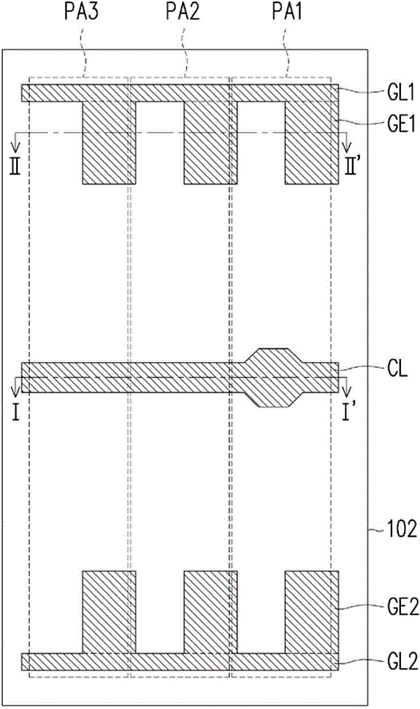
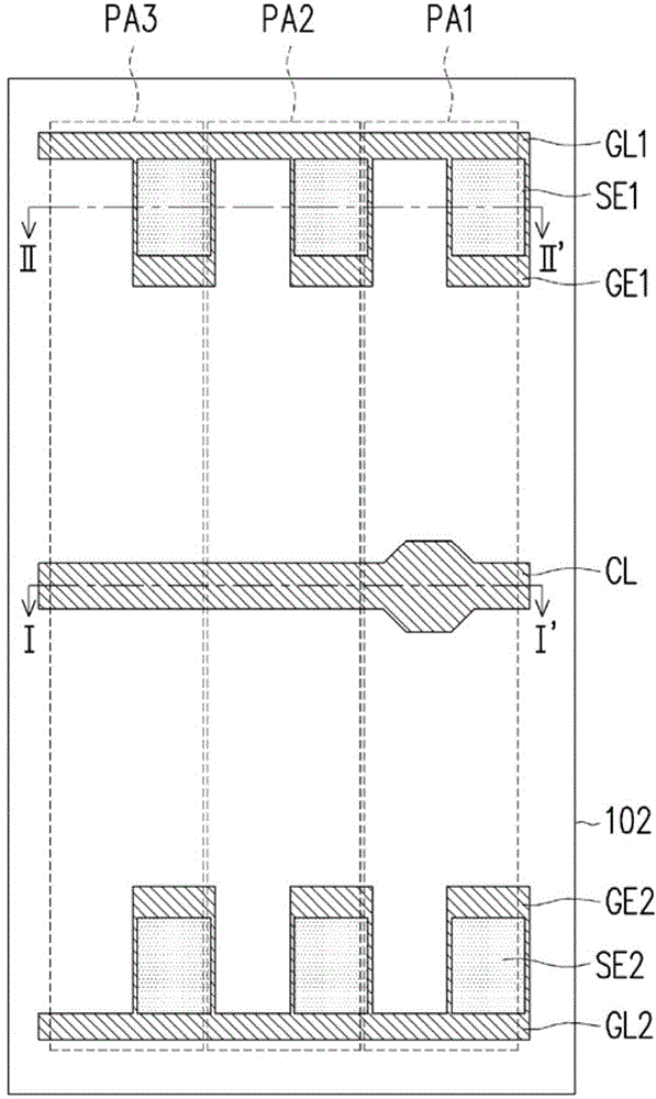
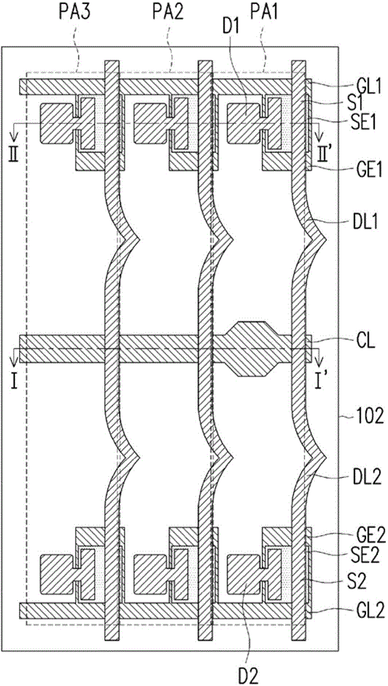
[0059] Figure 1A to Figure 1E It is a schematic top view of the process flow of the manufacturing method of the pixel structure according to an embodiment of the present invention, Figure 2A to Figure 2E for along Figure 1A to Figure 1E A schematic cross-sectional view of I-I', and Figure 3A to Figure 3E for along Figure 1A to Figure 1EThe schematic cross-section of II-II'. In particular, for the sake of clarity, three pixel areas are taken as an example in the drawings for illustration, but the present invention is not limited thereto. Please also refer to Figure 1A , Figure 2A as well as Figure 3A , firstly, a first gate line GL1, a second gate line GL2, a first gate GE1, a second gate GE2 and a connection line CL are formed on a substrate 102, wherein the first gate GE1 and the second gate GE2 are located on both sides of the connection line CL and between the first gate line GL1 and the second gate line GL2 . Specifically, a first conductor layer (not shown) i...


PUM


Abstract

A method of fabricating a pixel structure is provided. First and second gate lines, first and second gates and a connecting line are formed on the substrate, wherein the first and second gates are disposed at two sides of the connecting line and between the first and second gate lines. A gate insulating layer is formed. First and second semiconductor layers are respectively formed on the gate insulating layer above the first and second gates. First and second source/drain regions are formed respectively on the opposite sides of the first and second semiconductor layers, and drain lines are formed on substrate. An insulating layer having an opening is formed on the substrate, and the opening is disposed above and exposes the connecting line. A common electrode is formed on the insulating layer and electrically connects to the connecting line through the opening. First and second pixel electrodes are formed on the common electrode and electrically connect to the first and second drain regions respectively.

Description

technical field [0001] The present invention relates to an element and its manufacturing method, and in particular to a pixel structure and its manufacturing method. Background technique [0002] In recent years, with the maturity of optoelectronic technology and semiconductor manufacturing technology, the flat panel display (FlatPanelDisplay) has been vigorously developed. Liquid crystal displays have the advantages of low-voltage operation, no radiation scattering, light weight, and small size. Therefore, they gradually replace traditional cathode ray tube displays and become the mainstream of display products in recent years. However, liquid crystal displays still have the problem of limited viewing angles. At present, the technologies that can meet the requirement of wide viewing angle include twisted nematic (twistednematic, TN) liquid crystal plus wide viewing film (wideviewing film), in-plane switching (IPS) liquid crystal display, fringe field switching (FringeField...

Claims


Application Information

Patent Timeline
Patent Type & Authority Applications(China)
IPC IPC(8): H01L21/77H01L27/12H01L29/423H01L23/528G02F1/1333
Inventor 郭智宇
Owner CHUNGHWA PICTURE TUBES LTD
Why Eureka
Try Eureka