Pixel structure

A technology of pixel structure and pixel electrode, which is applied in nonlinear optics, instruments, optics, etc., and can solve the problems of unclear tilting direction of liquid crystal molecules, black streaks, light leakage, etc.

Active Publication Date: 2010-06-09
AU OPTRONICS CORP
View PDF0 Cites 17 Cited by
  • Summary
  • Abstract
  • Description
  • Claims
  • Application Information

AI Technical Summary

Problems solved by technology

However, the orientation of the liquid crystal molecules around the alignment bumps and the alignment slits is often unclear (disclination), resulting in light leakage or black streaks, which further reduces the display co

Method used


Image

  • Pixel structure
  • Pixel structure
  • Pixel structure

Examples


no. 1 example

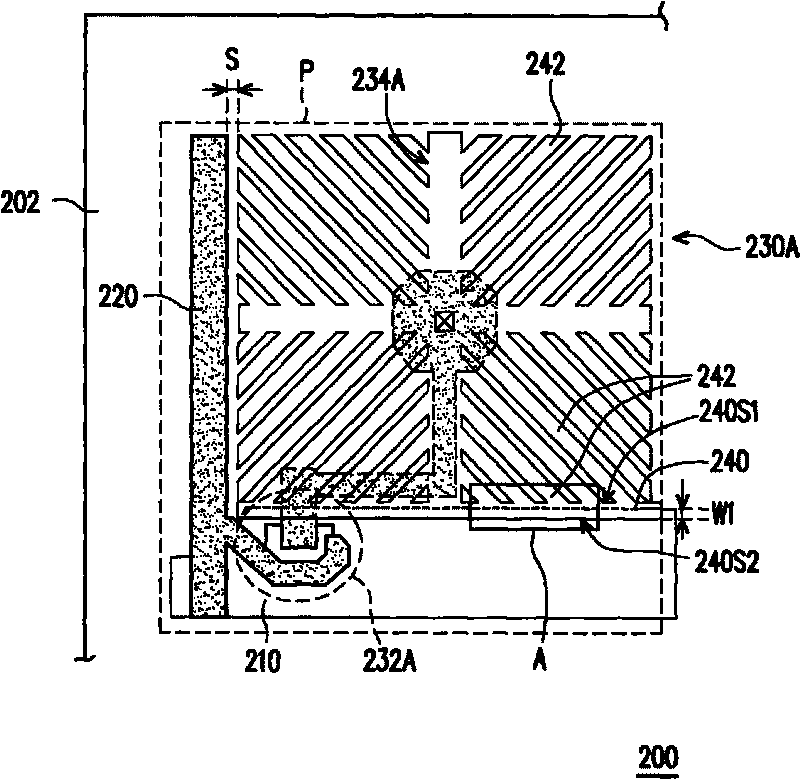
[0070] figure 1 It is a schematic diagram of the pixel structure of the first embodiment of the present invention. Please refer to figure 1 , the pixel structure 200 is disposed on a substrate 202 to define a plurality of pixel regions P on the substrate 202, wherein in order to clearly illustrate the relevant components in the pixel structure 200, in figure 1 The pixel structure 200 located in a pixel region P is only schematically shown in FIG. 2 as a representative illustration.

[0071] Please refer to figure 1 The pixel structure 200 includes a scan line 210 , a first data line 220 and a first pixel unit 230A disposed on a substrate 202 . In this embodiment, the first pixel unit 230A includes a first active element 232A and a first pixel electrode 234A, wherein the first active element 232A is electrically connected to the scan line 210 and the first data line 220 . The first pixel electrode 234A is electrically connected to the first active element 232A, and the firs...

no. 2 example

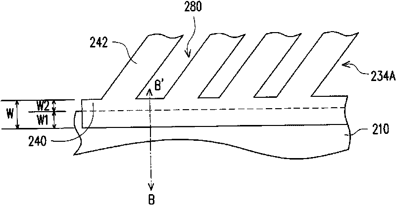
[0077] image 3 It is a partially enlarged schematic diagram of a pixel structure according to the second embodiment of the present invention. Please refer to image 3 In the pixel structure 300 of this embodiment, the first pixel unit 330A is similar to the first pixel unit 230A of the first embodiment, but the first pixel unit 330A of this embodiment further includes a storage capacitor structure 260 .

[0078] Specifically, as image 3 As shown, the first pixel electrode 234A has a main portion 310 parallel to the first data line 220 and a branch portion 320 parallel to the scan line 210 . The main body 310 and the branch 320 divide the first pixel unit 330A into four regions R1, R2, R3, R4, and a plurality of branches 242 extend around the intersection of the main body 310 and the branch 320, and divide the pixel unit into four regions. There are three regions R1, R2, R3, R4, and the branches 242 in each region R1, R2, R3, R4 are substantially parallel to each other. W...

no. 3 example

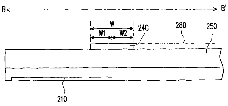
[0082] Figure 4A is a top view of a pixel structure in the third embodiment of the present invention, and Figure 4B for Figure 4A The partially enlarged schematic diagram of the pixel structure. Please refer to Figure 4A and Figure 4B The pixel structure 400 of this embodiment is similar to the foregoing embodiments, but the first pixel unit 430A of the pixel structure 400 of this embodiment further includes a color filter located between the first active element 232A and the first pixel electrode 234A. The optical layer 250, for clarity, the color filter layer 250 is automatically Figure 4A Extracted from the left side of and shown separately in Figure 4A to the right of the .

[0083] Please refer to Figure 4A and Figure 4B , in this embodiment, the pixel structure 400 belongs to the pixel structure 400 in which the color filter film is directly integrated on the thin film transistor array substrate. Such as Figure 4A and Figure 4B As shown, the color f...


PUM


Abstract

The invention relates to a pixel structure, which comprises a substrate, a scanning line, a first data wire and a first pixel unit, wherein the scanning line and the first data wire are arranged on the substrate; the first pixel unit comprises a first active element and a first pixel electrode; the first active element, the scanning line and the first data wire are electrically connected; the first pixel electrode is electrically connected with the first active element; the first pixel electrode is provided with a strip pattern which is parallel to the scanning line in general and a plurality of branches which are electrically connected with the strip pattern; one side of the strip pattern is connected with the branches extending to the scanning line, and the other side of the strip pattern is overlapped with part of the scanning line; and the overlapped width of the strip pattern and the scanning line is 40 to 90 percent of the width of the strip pattern. Therefore, the pixel structure has high aperture opening ratio, and can obtain good display quality.

Description

technical field [0001] The present invention relates to a pixel structure, and in particular to a pixel structure capable of improving display quality. Background technique [0002] The performance requirements of the market for LCD panels are towards high contrast ratio, no gray scale inversion, little color shift, high luminance, high color richness, Features such as high color saturation, fast response and wide viewing angle. At present, the technologies that can meet the requirement of wide viewing angle include twist nematic (TN) liquid crystal plus wide viewing film (wide viewing film), in-plane switching (IPS) liquid crystal display panel, fringe field A fringe field switching liquid crystal display panel, a multi-domain vertically aligned (MVA) liquid crystal display panel, and the like. [0003] The known multi-domain vertical alignment liquid crystal display panel utilizes the configuration of the alignment structure to make the liquid crystal molecules in differ...

Claims


Application Information

Patent Timeline
IPC IPC(8): G02F1/1362
Inventor 郑为元曾庆安黄彦衡白佳蕙陈宗凯曾文贤卓庭毅李佳育
Owner AU OPTRONICS CORP
Why Eureka
Try Eureka