contact image sensor

An image sensor and contact technology, applied in the field of image sensors, can solve problems such as the complex and bulky structure of the contact image sensor, and achieve the effect of improving the imaging quality

Active Publication Date: 2018-12-11
SHANGHAI OXI TECH
View PDF6 Cites 0 Cited by
  • Summary
  • Abstract
  • Description
  • Claims
  • Application Information

AI Technical Summary

Problems solved by technology

from figure 1 It can be seen intuitively that the overall structure of the existing contact image sensor is complex and bulky

Method used


Image

  • contact image sensor
  • contact image sensor
  • contact image sensor

Examples


Embodiment Construction

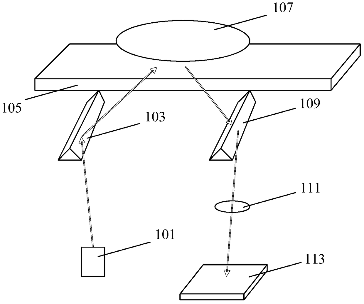
[0033] When the contact image sensor performs image acquisition, the object to be collected is closely attached to the surface of the image sensor, and the external light source cannot shine on the object and the surface of the sensor through the opaque object. Moreover, in order to ensure that the image sensor chip only receives light reflected from objects, it is required that the back of the pixel of the image sensor chip cannot transmit light, that is, the light cannot directly irradiate the pixels on the surface of the image sensor chip from the back of the image sensor chip. Therefore, existing contact image sensors usually use figure 1 The complex structure shown. However, this complex structure is bulky and thick, which does not conform to the trend of thinner and lighter electronic products, and it is difficult to integrate this complex structure with other electronic products, so its application is greatly limited.

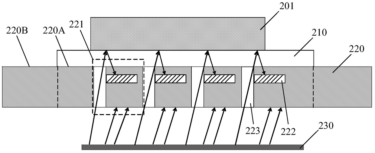
[0034] To this end, the present invention provide...


PUM


Abstract

The invention provides a contact image sensor, which comprises a protective layer, a backlight source and an image sensor chip, wherein the image sensor chip is located between the protective layer and the backlight source; the surface of the image sensor chip comprises a pixel array region and a peripheral region; the peripheral region surrounds the pixel array region; at least one of the pixel array region and the peripheral region comprises a through hole region; the through hole region comprises a through hole which runs through the thickness of the image sensor chip; and light emitted from the backlight source passes through the image sensor chip via the through hole and reaches the protective layer. The thickness of the contact image sensor is reduced and the structure is simplified.

Description

technical field [0001] The invention relates to the field of image sensors, in particular to a contact image sensor. Background technique [0002] When the contact image sensor performs image acquisition, when the collected object is close to the surface of the contact image sensor, the external light source cannot shine through the opaque object to the object and the surface of the contact image sensor, so an effective photoelectric response cannot be formed. To this end, complex light paths must be used to achieve illumination of the object to be acquired. [0003] A Complementary Metal Oxide Semiconductor (CMOS) image sensor chip is a semiconductor device that converts light signals into electrical signals. CMOS image sensor chips have many advantages. Its photosensitive element (ie pixel) can achieve very sensitive light response. When the light intensity is very weak, a large photoelectric signal can be generated, which is much larger than the noise in the system. T...

Claims


Application Information

Patent Timeline
Patent Type & Authority Patents(China)
IPC IPC(8): H01L27/146
Inventor 朱虹林崴平
Owner SHANGHAI OXI TECH
Why Eureka
Try Eureka