Formation method of semiconductor structure

A semiconductor and layer-forming technology, used in semiconductor/solid-state device manufacturing, electrical components, circuits, etc., and can solve the problem of high failure rate

Active Publication Date: 2018-12-21
SEMICON MFG INT (SHANGHAI) CORP
View PDF2 Cites 0 Cited by
  • Summary
  • Abstract
  • Description
  • Claims
  • Application Information

AI Technical Summary

Problems solved by technology

[0004] However, after the high aspect ratio process is used to form the interlayer dielectric layer on the above-mentioned stress layer, no matter in the production line or offline, when the wafer is trouble shooting, the failure rate is too high. Obsession is especially acute when detecting particulate matter problems

Method used


Image

  • Formation method of semiconductor structure
  • Formation method of semiconductor structure
  • Formation method of semiconductor structure

Examples


Embodiment Construction

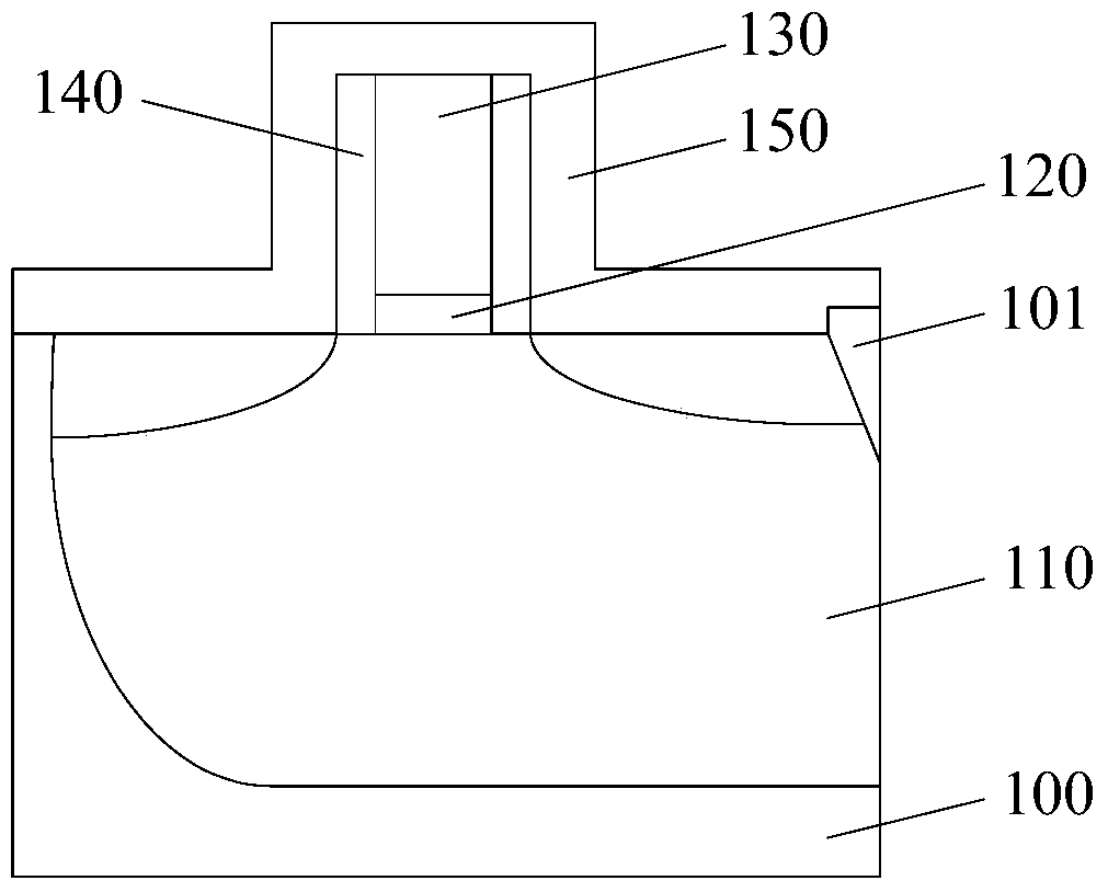
[0024] As mentioned in the background technology, after the existing method uses a high aspect ratio process to form the upper stress layer interlayer dielectric layer, when performing fault detection, the failure rate is too high. This problem is manifested in the detection of particulate matter problems. particularly serious.

[0025] Analyzing the reason, the structure of the interlayer dielectric layer formed by the high aspect ratio process is relatively soft, and the surface roughness is relatively large, which leads to the situation that the rough surface is mistakenly detected as particles in the detection of particle problems, resulting in a failure rate during fault detection. Excessively bothered.

[0026] Further analysis of the reason for the large surface roughness of the interlayer dielectric layer found that the formation material of the interlayer dielectric layer is usually tetraethyl silicate. When the high aspect ratio process directly forms the interlayer ...


PUM


Abstract

Provided is a formation method of a semiconductor structure. The method includes: a grid stacking structure is formed on a semiconductor substrate; a stress layer covering the grid stacking structure is formed on the semiconductor substrate; ozone plasma processing of the surface of the stress layer is performed so that an oxidation thin layer is formed on the surface of the stress layer; and after the ozone plasma processing, an interlayer dielectric layer is formed on the stress layer. According to the method, the problem of over-high failure rate during fault detection of wafers can be eliminated.

Description

technical field [0001] The invention relates to the field of semiconductor manufacturing, in particular to a method for forming a semiconductor structure. Background technique [0002] In the manufacture of semiconductor devices, the stress layer can be used to induce stress in the transistor channel, thereby adjusting the carrier mobility in the channel. Complementary Metal-Oxide-Semiconductor (CMOS) structures include NMOS structures and PMOS structures. For CMOS structures, it is necessary to deposit a stress layer with tensile stress (tensile stress) on the NMOS structure. In the PMOS structure A stress layer with compressive stress is deposited on it, and the stress layer is usually made of silicon nitride. [0003] With the reduction of the geometric size of the semiconductor structure, the high aspect ratio process (High Aspect Ratio Process, HARP) is used to form the interlayer dielectric layer to improve the gap filling (gap) of the interlayer dielectric layer (int...

Claims


Application Information

Patent Timeline
Patent Type & Authority Patents(China)
IPC IPC(8): H01L21/336
Inventor 周洁鹏陈志刚
Owner SEMICON MFG INT (SHANGHAI) CORP
Why Eureka
Try Eureka