Magnetic shielding package of non-volatile magnetic memory element

一种非易失性、磁存储的技术,应用在非易失性磁存储元件的磁屏蔽封装体领域,能够解决增加MRAM的磁场危险性等问题,达到低成本、屏蔽效果提高的效果

Active Publication Date: 2016-06-22
AMKOR TECH JAPAN INC
View PDF8 Cites 4 Cited by
  • Summary
  • Abstract
  • Description
  • Claims
  • Application Information

AI Technical Summary

Problems solved by technology

[0016] In addition, in the magnetic shield structure described in Patent Document 1, the magnetic body is in contact with the MRAM chip. Although it is considered to be effective for high-frequency magnetic fields, there is an increase in reach because the magnetic flux is concentrated in the magnetic body region for static and low-frequency magnetic fields. Dangers of Magnetic Fields in MRAM

Method used


Image

  • Magnetic shielding package of non-volatile magnetic memory element
  • Magnetic shielding package of non-volatile magnetic memory element
  • Magnetic shielding package of non-volatile magnetic memory element

Examples


Embodiment approach 1

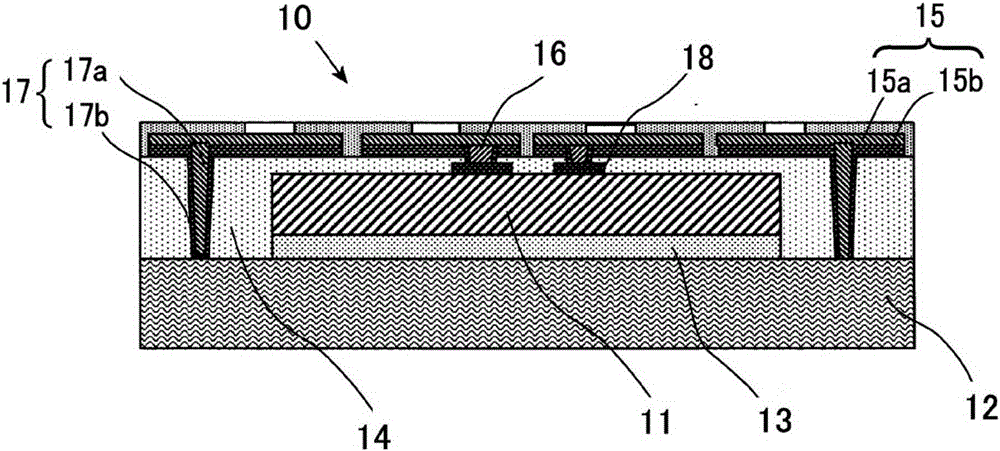
[0059] exist figure 1 The structure of the magnetic shield package of Embodiment 1 is shown in .

[0060] figure 1 It is a vertical cross-sectional view of a magnetic shield package (hereinafter also simply referred to as "magnetic shield package") of the nonvolatile magnetic memory element according to the present invention.

[0061] figure 1 The magnetic shielding package 10 shown in has: a nonvolatile magnetic storage element 11 having an electrode 18; a support plate 12 comprising a soft magnetic material; a first insulating material layer 13; a second insulating material layer 14; a wiring layer 15 ; the conductive portion 16 ; and the magnetic shield member 17 .

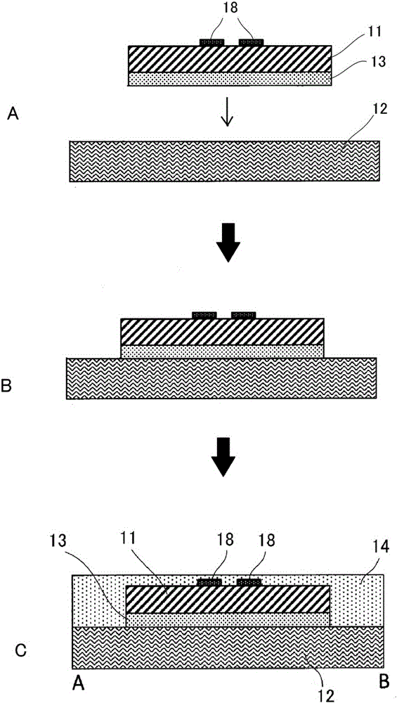
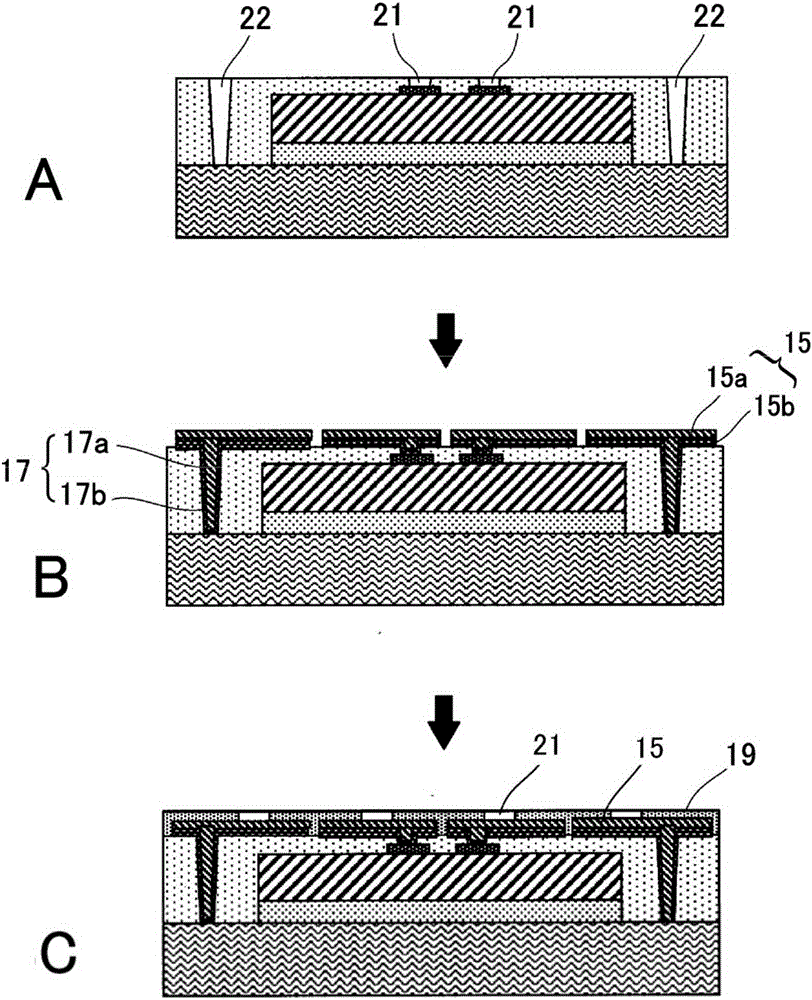
[0062] The nonvolatile magnetic memory element 11 is adhered and fixed on the first insulating material layer 13 formed on the support plate 12 . The nonvolatile magnetic memory element 11 and its periphery are sealed with a second insulating material layer 14 . Wiring layer 15 has a laminated structure...

Embodiment approach 2

[0093] Figure 7 The structure of the magnetic shield package of Embodiment 2 is shown in .

[0094] In Embodiment 1, the wiring layer has a laminated structure including the conductor layer 15a and the soft magnetic layer 15b, but in this embodiment, as Figure 7 As shown, the conductor layer and the soft magnetic layer are separated, and the conductor layer and the soft magnetic layer are provided as independent layers in the second insulating material layer 14 as the wiring layer 15 and the soft magnetic layer 25 . In the soft magnetic layer 25 , an opening 26 is provided in a portion where the conductive portion 16 is disposed.

[0095] With such a structure, since the upper surface of the MRAM can be completely covered with the soft magnetic layer except the portion where the opening 26 of the conductive portion 16 is arranged, the effect of shielding the static magnetic field and the low-frequency magnetic field is improved.

[0096] The conductor layer 15 and the soft...

Embodiment approach 3

[0112] Figure 9 The structure of the magnetic shield package of Embodiment 3 is shown in .

[0113] In this embodiment, a magnetic shield package is formed using the support plate 12 having the cavity 29 .

[0114] In the cavity 29, the MRAM 11 is sealed by the second insulating material layer 14a.

[0115] On the upper surface of the second insulating material layer 14a, with Figure 8 In the magnetic shield package shown, likewise, the soft magnetic layer 25 including the foil 25' is laminated and sealed with the second insulating material layer 14b.

[0116] The soft magnetic layer 25 is magnetically connected to the support plate 12 through the connecting portion 30 .

[0117] In this embodiment, since the side wall part of the support plate 12 having the cavity 29 is used as the magnetic shielding layer, by thickening the side wall of the support plate 12, a higher static magnetic field and low frequency magnetic field shielding effect can be obtained.

[0118]

[...


PUM


Abstract

A magnetic shielding package of a non-volatile magnetic memory element, including: a soft magnetic material support plate (12); a first insulating material layer (13) formed on the support plate; a non-volatile magnetic memory element (11) fixed on the first insulating material layer; a second insulating material layer (14) that encapsulates the memory element and the periphery thereof; in the second insulating material layer, a wiring layer (15), a soft magnetic layer (15b) or (25) and a conductive portion (16) connecting an electrode of the circuit surface of the memory element and the wiring layer; and a magnetic shield part (17) containing a soft magnetic material arranged like a wall with a distance from a side surface of the memory element so as to surround the memory element side surface partially or entirely, the magnetic shield part being magnetically connected to the soft magnetic layer.

Description

technical field [0001] The present invention relates to a magnetic shielding package of a nonvolatile magnetic storage element, in particular to a magnetic shielding package of a nonvolatile magnetic storage element for suppressing the influence of an external magnetic field on the nonvolatile magnetic storage element. Background technique [0002] MRAM (Magnetoresistive Random Access Memory: magnetoresistive random access memory), which is a memory using a magnetic body, is a non-volatile memory that can hold data without external power supply, so it does not require standby power and has unlimited rewrite resistance. And / or high-speed, low-power consumption, and large-capacity memories are expected. [0003] However, since the basic element of MRAM stores information in the direction of spontaneous magnetization of the magnetic material, if an external magnetic field of about 10 to 50 [Oe], which is the antiphase magnetic field strength of the MRAM element, is irradiated, ...

Claims


Application Information

Patent Timeline
Patent Type & Authority Applications(China)
IPC IPC(8): H01L27/22H01L43/08
CPCH01L24/19H01L24/20H01L24/97H01L2224/04105H01L2224/32245H01L2224/73267H01L2224/92244H01L2224/97H01L2924/15153H01L2224/8203H01L23/552H01L2224/83
Inventor 松原宽明岩崎俊宽近井智哉石堂仁则渡边真司玉川道昭
Owner AMKOR TECH JAPAN INC
Why Eureka
Try Eureka