
Integrated Fan-Out Structure with Openings in Buffer Layer

A technology of buffer layer and laminated film, applied in the direction of electrical components, electrical solid devices, circuits, etc., can solve the problem of limiting the number of solder balls

Active Publication Date: 2016-06-29
TAIWAN SEMICON MFG CO LTD
View PDF5 Cites 2 Cited by
  • Summary
  • Abstract
  • Description
  • Claims
  • Application Information

AI Technical Summary

Problems solved by technology

Therefore, under the condition that the solder ball size is required to be fixed, the solder ball must be of a specific size, which in turn limits the number of solder balls that can be packaged onto the die surface

Method used


Image

  • Integrated Fan-Out Structure with Openings in Buffer Layer
  • Integrated Fan-Out Structure with Openings in Buffer Layer
  • Integrated Fan-Out Structure with Openings in Buffer Layer

Examples


Embodiment Construction

[0033] The making and using of embodiments of the present disclosure are discussed in detail below. It should be appreciated, however, that the embodiments provide many applicable concepts that can be embodied under various specific conditions. The specific embodiments discussed are illustrative and do not limit the scope of the disclosure.

[0034] Integrated fan-out (InFO) packages including vias and methods of forming the same are provided according to various exemplary embodiments. Intermediate stages in forming the InFO package are shown. Variations of the examples are discussed. Like reference numerals are used to refer to like elements in the various views and illustrated embodiments.

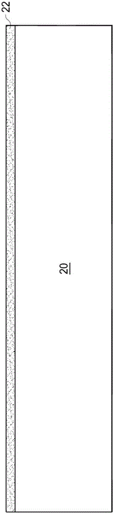
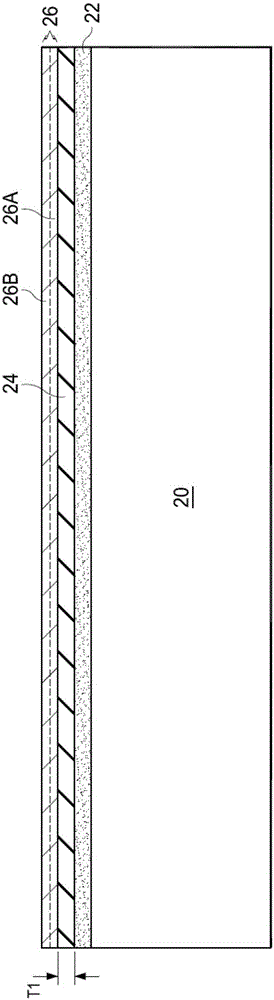
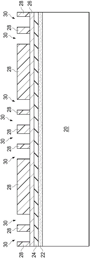
[0035] Figure 1 to Figure 12 , Figure 13A , Figure 14A , Figure 15 with Figure 16 is a cross-sectional view of an intermediate stage of manufacturing a package structure according to some example embodiments. refer to figure 1 , the carrier 20 is set, and the adhesive laye...


PUM

PropertyMeasurementUnit
Heightaaaaaaaaaa
The average diameteraaaaaaaaaa

Abstract

A package includes a molding compound, a through-via penetrating through the molding compound, a device die molded in the molding compound, and a buffer layer on and contacting the molding compound. An opening is through the buffer layer to the through-via. The buffer layer has ripples in a plane parallel to an interface between the molding compound and the buffer layer and around a circumference of the opening. Other embodiments contemplate an additional package bonded to the package, and methods for forming the package.

Description

[0001] This application is a continuation-in-part of US Patent Application Serial No. 14 / 024,311, filed September 11, 2013, entitled "Integrated Fan-Out Structure with Guiding Trenches in Buffer Layer," the entire contents of which are hereby incorporated by reference. technical field [0002] The present invention generally relates to the field of semiconductors, and more particularly, to packaging of semiconductors. Background technique [0003] As semiconductor technology develops, semiconductor chips / die become smaller and smaller. At the same time, more functions need to be integrated into the semiconductor die. As a result, semiconductor dies need to pack more and more I / O pads into a smaller area, so the density of I / O pads increases rapidly over time. As a result, packaging of the semiconductor die becomes more difficult, which can adversely affect packaging yield. [0004] Conventional packaging techniques can be divided into two categories. In the first category...

Claims


Application Information

Patent Timeline
IPC IPC(8): H01L23/31H01L21/56
CPCH01L24/19H01L21/6836H01L24/97H01L25/105H01L25/50H01L2224/04042H01L2224/04105H01L2224/12105H01L2224/16227H01L2224/32145H01L2224/32225H01L2224/48091H01L2224/48229H01L2224/73265H01L2224/73267H01L2224/92244H01L2224/97H01L2225/0651H01L2225/1035H01L2225/1041H01L2225/1064H01L2225/1082H01L2924/15311H01L2924/1815H01L2225/06568H01L2924/181H01L21/6835H01L2221/68327H01L2221/68359H01L23/3128H01L24/16H01L24/32H01L24/48H01L24/73H01L24/83H01L2924/1431H01L2924/1432H01L2924/00014H01L21/4853H01L23/5389H01L2224/19H01L2224/83H01L2224/48227H01L2924/00012H01L2224/45099H01L2224/45015H01L2924/207H01L2224/83005
Inventor 邱梧森郑礼辉蔡柏豪林俊成
Owner TAIWAN SEMICON MFG CO LTD
Features
  • Generate Ideas
  • Intellectual Property
  • Life Sciences
  • Materials
  • Tech Scout
  • Unparalleled Data Quality
  • Higher Quality Content
  • 60% Fewer Hallucinations
Learn More