Nitride based transistors on semi-insulating silicon carbide substrates

a silicon carbide substrate and nitride technology, applied in the direction of semiconductor devices, electrical equipment, basic electric elements, etc., can solve the problems that more familiar semiconductor materials have not been able to penetrate higher power high frequency applications to the extent desirable, and achieve the effect of high electron mobility

Inactive Publication Date: 2001-11-13
WOLFSPEED INC
View PDF8 Cites 820 Cited by
  • Summary
  • Abstract
  • Description
  • Claims
  • Application Information

AI Technical Summary

Benefits of technology

An aluminum nitride buffer layer 12 is on the substrate 11 and provides an appropriate crystal structure transition between the silicon carbide substrate and the remainder of the transistor. Silicon carbide has a much closer crystal lattice match to Group III nitrides than does sapphire (Al.sub.2 O.sub.3) which is a very common substrate material for Group III nitride devices. The closer lattice match results in Group III nitride films of higher quality than those generally available on sapphire. Perhaps most importantly, silicon carbide also has a very high thermal conductivity so that the total output power of Group III nitride devices on silicon carbide is not as limited by thermal dissipation of the substrate as in the case of the same devices formed on sapphire. Also, the availability of semi-insulating silicon carbide substrates provide the capacity for device isolation and reduced parasitic capacitance that make workable commercial devices feasible.
In preferred embodiments of the invention, the source and drain contacts 20 and 21 are preferably formed of alloys of titanium, aluminum, and nickel, and the rectifying gate contact is preferably selected from the group consisting of titanium, platinum, chromium, alloys of titanium and tungsten, and platinum silicide. In a particularly preferred embodiment, the ohmic contacts are formed of an alloy of nickel, silicon, and titanium that is formed by depositing respective layers of these materials, and then annealing them. Because this alloy system eliminates aluminum, it avoids unwanted aluminum contamination over the device surface when the anneal temperature exceeds the melting point of aluminum (660.degree. C.).

Problems solved by technology

These more familiar semiconductor materials have failed to penetrate higher power high frequency applications to the extent desirable, however, because of their relatively small bandgaps (e.g., 1.12 eV for Si and 1.42 for GaAs at room temperature) and relatively small breakdown voltages.

Method used


Image

  • Nitride based transistors on semi-insulating silicon carbide substrates
  • Nitride based transistors on semi-insulating silicon carbide substrates
  • Nitride based transistors on semi-insulating silicon carbide substrates

Examples


Embodiment Construction

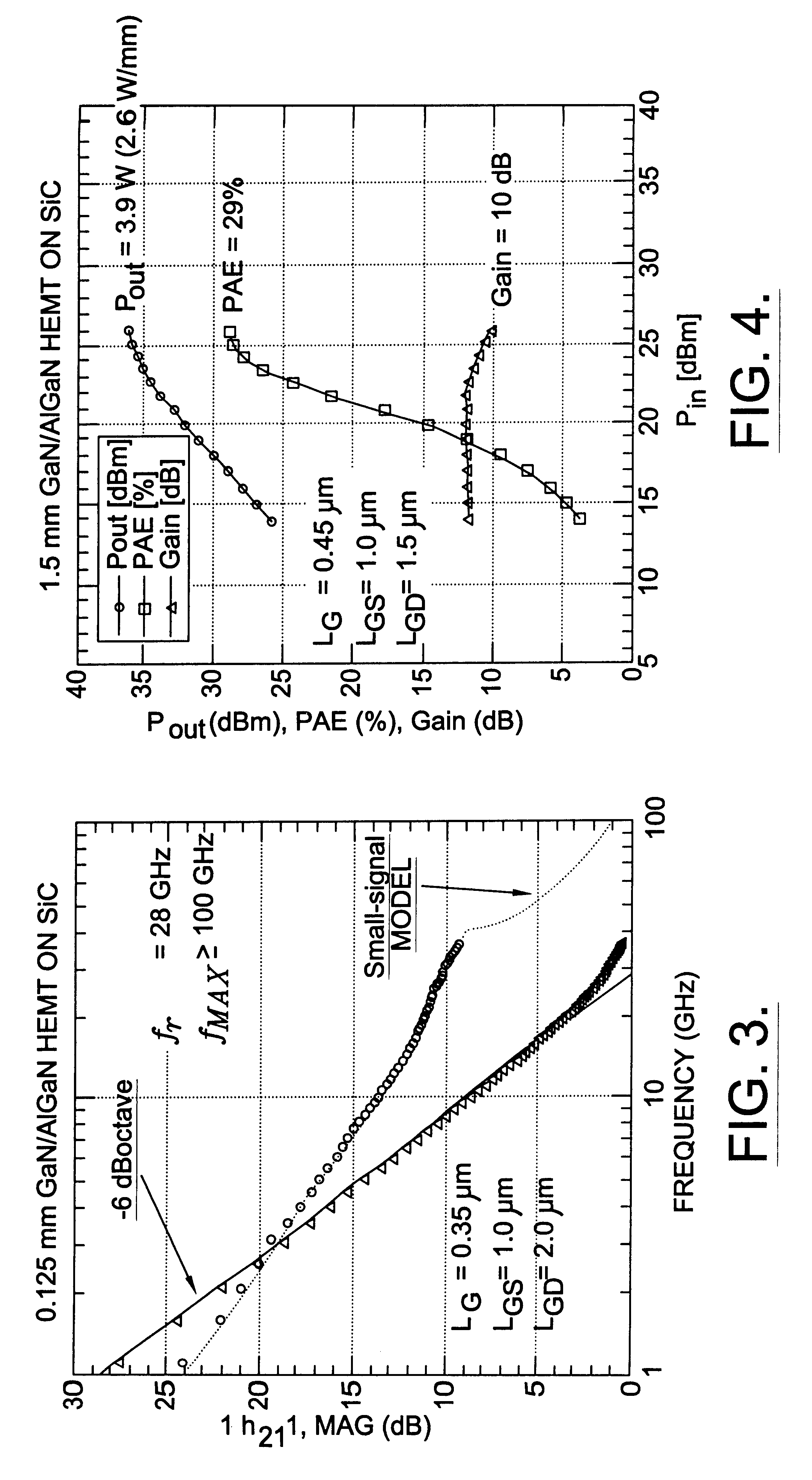
In the present invention, GaN / AlGaN HEMTs fabricated on semi-insulating 4H silicon carbide substrates have shown a total output power of 4 Watts CW (2.0 W / mm) at 10 GHz and -1 dB gain compression from a 2 mm gate width (16.times.125 .mu.m) with a power added efficiency of 29% and an associated gain of 10 dB. To date, this represents the highest total power and associated gain demonstrated for a III-Nitride HEMT at X-Band.

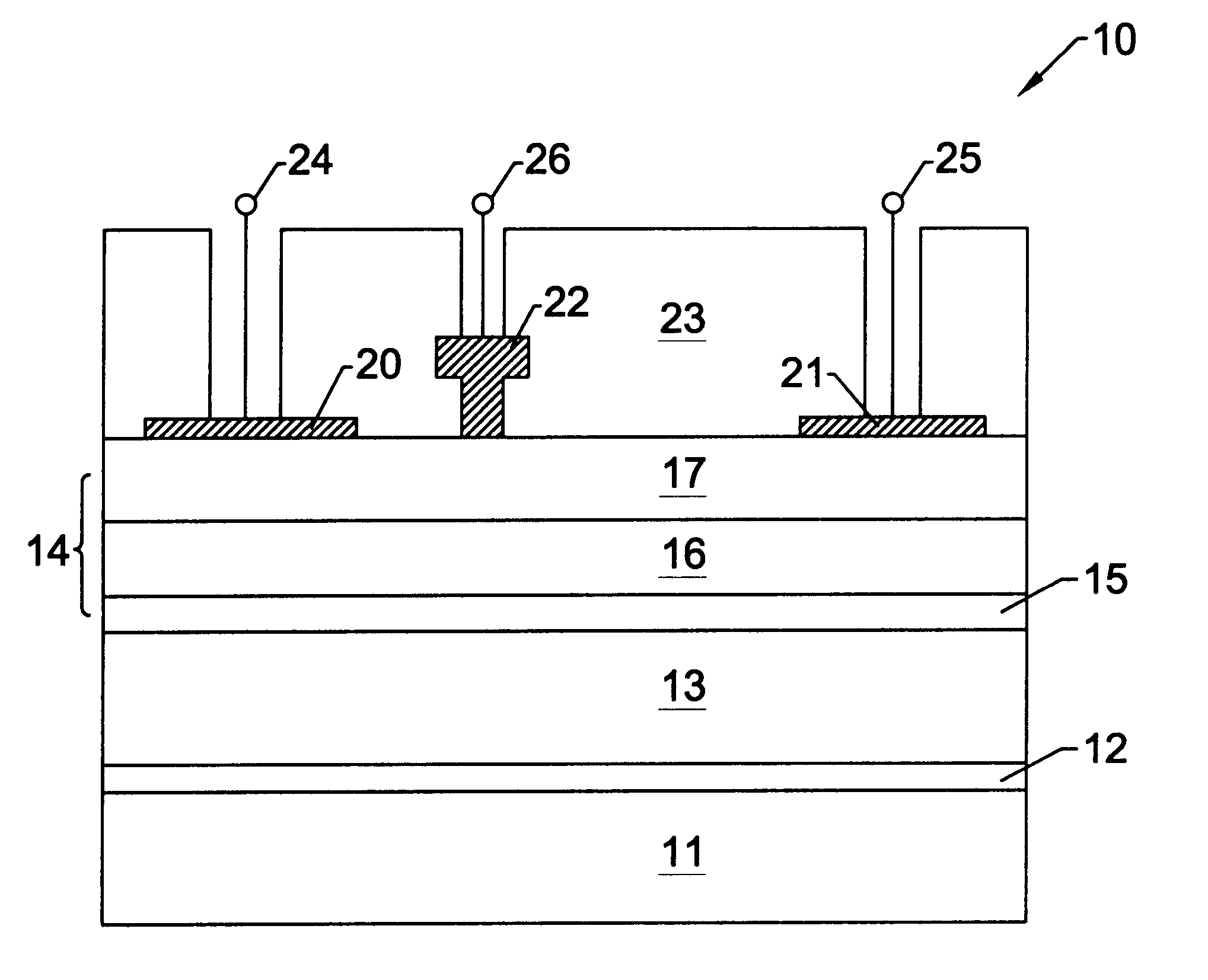
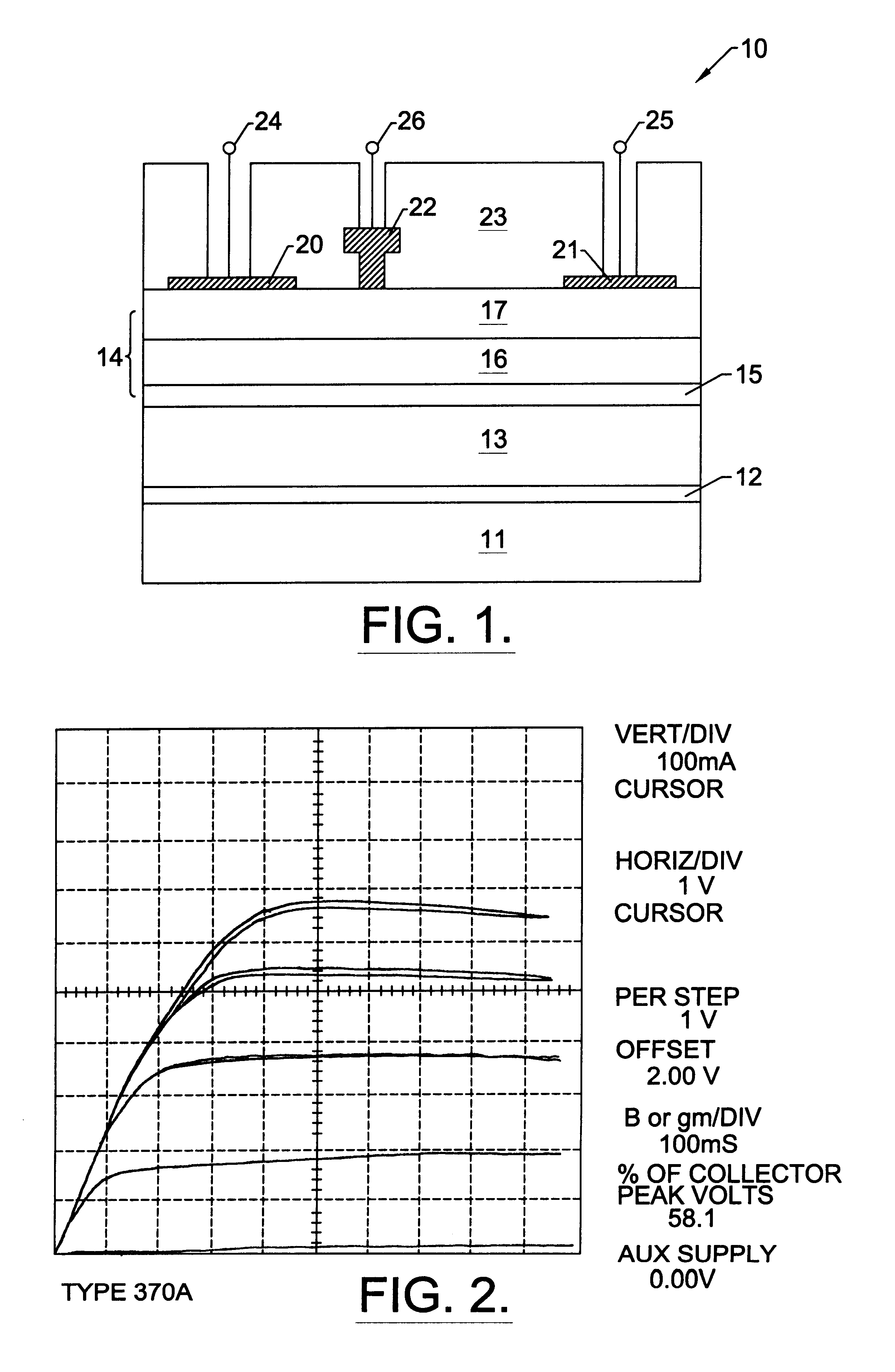
As shown in FIG. 1, the epilayer structure is comprised of an AlN Buffer Layer, 2 .mu.m of undoped GaN, and 27 nm of Al.sub.0.14 Ga.sub.0.86 N. The AlGaN cap has a 5 nm undoped spacer layer, a 12 nm donor layer, and a 10 nm undoped barrier layer. Device isolation was achieved with mesa etching. Ohmic contacts were Ti / Al / Ni contacts annealed at 900.degree. C. Across a 35 mm diameter SiC wafer, average values of contact resistance and sheet resistance were 0.36 .OMEGA.-mm and 652 .OMEGA. / square, respectively, showing the high quality of the 2DEG over a large area.

Typi...


PUM

PropertyMeasurementUnit
total output poweraaaaaaaaaa
thicknessaaaaaaaaaa
thicknessaaaaaaaaaa

Abstract

A high electron mobility transistor (HEMT) is disclosed that includes a semi-insulating silicon carbide substrate, an aluminum nitride buffer layer on the substrate, an insulating gallium nitride layer on the buffer layer, an active structure of aluminum gallium nitride on the gallium nitride layer, a passivation layer on the aluminum gallium nitride active structure, and respective source, drain and gate contacts to the aluminum gallium nitride active structure.

Description

The present invention relates to high frequency transistors and in particular relates to a high electron mobility transistor (HEMT) that incorporates nitride-based active layers and a silicon carbide substrate.The present invention relates to transistors formed of semiconductor materials that make them suitable for high power, high temperature, and high frequency applications. As known to those familiar with semiconductors, materials such as silicon (Si) and gallium arsenide (GaAs) have found wide application in semiconductor devices for lower power and (in the case of Si) lower frequency applications. These more familiar semiconductor materials have failed to penetrate higher power high frequency applications to the extent desirable, however, because of their relatively small bandgaps (e.g., 1.12 eV for Si and 1.42 for GaAs at room temperature) and relatively small breakdown voltages.Accordingly, interest in high power high temperature and high frequency applications and devices ha...

Claims


Application Information

Patent Timeline
Patent Type & Authority Patents(United States)
IPC IPC(8): H01L29/267H01L29/02H01L29/66H01L29/778H01L29/45H01L29/40H01L29/24H01L29/20H01L29/26H01L21/338H01L29/812
CPCH01L29/1608H01L29/267H01L29/452H01L29/7783H01L29/7787H01L29/2003H01L29/778
Inventor SHEPPARD, SCOTT THOMASALLEN, SCOTT THOMASPALMOUR, JOHN WILLIAMS
Owner WOLFSPEED INC
Why Eureka
Try Eureka