Display mother board, manufacturing method of display mother board, display panel and display device

A technology for display substrates and display panels, which is used in identification devices, nonlinear optics, instruments, etc., can solve the problems of the sealant 11 being enlarged, affecting mass production, blank bubbles, etc., so as to improve the cutting yield and reduce the ratio of light leakage at four corners. , the effect of increasing the possibility of mass production

Inactive Publication Date: 2016-07-27
BOE TECH GRP CO LTD +1
View PDF5 Cites 3 Cited by
  • Summary
  • Abstract
  • Description
  • Claims
  • Application Information

AI Technical Summary

Problems solved by technology

[0003] In the existing technology, such as figure 1 As shown, for the coating of the sealant 11 of each display substrate 10 on the same display motherboard 1, the method of coating the sealing area of ​​each display substrate 10 is usually adopted, and this coating makes the display substrate The sealant 11 at the four corners of 10 is relatively thick, which will cause light leakage at the corners and seriously affect the possibility of mass production
like figure 2 As shown, when this sealant 11 is used to coat the display substrate 10 with zero cut (the so-called zero cut refers to: the cutter wheel cuts directly to the glue) display substrate 10, blank bubbles will appear at the corner where the two display substrates 10 meet. , that is, the phenomenon that the sealant 11 is not fully covered, which eventually leads to poor cutting of the display motherboard 1

Method used


Image

  • Display mother board, manufacturing method of display mother board, display panel and display device
  • Display mother board, manufacturing method of display mother board, display panel and display device
  • Display mother board, manufacturing method of display mother board, display panel and display device

Examples


Embodiment 1

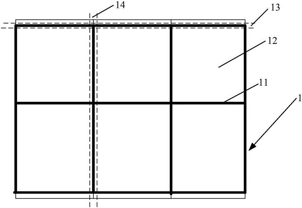
[0023] Such as image 3 As shown, this embodiment provides a method for preparing a display motherboard, wherein the display motherboard 1 includes multiple rows of first sealing regions 13 and multiple columns of second sealing regions 14, and the first sealing regions 13 and the second sealing regions The intersecting positions of the sealing areas 14 define a display area 12; the preparation method includes: applying the sealant 11 to the first sealing area 13 and the second sealing area 14 in a linear coating manner.

[0024] It should be noted that the coating sequence of the first sealing area 13 and the second sealing area 14 is not limited in this embodiment, that is, the first sealing area 13 can be coated sequentially and then the second sealing area 13 can be coated sequentially The second sealing area 14 may also be coated sequentially with the second sealing area 14 and then the first sealing area 13 , of course, the coating of the first sealing area 13 and the se...

Embodiment 2

[0033] This embodiment provides a display device, which includes the display panel in Embodiment 1. So its performance is better.

[0034] Of course, the display device in this embodiment can be any product or component with a display function, such as a mobile phone, a tablet computer, a television, a monitor, a notebook computer, a digital photo frame, a navigator, and the like.

[0035] Of course, the display device in this embodiment also has structures such as the outer frame of a conventional display device.


PUM


Abstract

The invention provides a display mother board, a manufacturing method of the display mother board, a display substrate, a manufacturing method of the display substrate, a display panel and a display device and belongs to the technical field of display. The display mother board comprises multiple rows of first sealed areas and multiple columns of second sealed areas, and the intersection positions of the first sealed areas and the second sealed areas define a display area. The manufacturing method of the display mother board comprises the step of coating the first sealed areas and the second sealed areas with a sealant in a linear coating mode. The manufacturing method of the display mother board can effectively prevent light leakage at four corners of the display substrate, and the yield of the display substrate formed through cutting is higher.

Description

technical field [0001] The invention belongs to the field of display technology, and in particular relates to a display motherboard and a preparation method thereof, a display substrate and a preparation method thereof, a display panel, and a display device. Background technique [0002] Currently, each individual display substrate is usually obtained by cutting a large display motherboard. A display area in the display motherboard corresponds to a display area of ​​a display substrate, and each display substrate also includes a sealing area surrounding the display area, and the display motherboard is between the sealing areas of two adjacent display substrates. cutting area. [0003] In the existing technology, such as figure 1 As shown, for the coating of the sealant 11 of each display substrate 10 on the same display motherboard 1, the method of coating the sealing area of ​​each display substrate 10 is usually adopted, and this coating makes the display substrate The ...

Claims


Application Information

Patent Timeline
Patent Type & Authority Applications(China)
IPC IPC(8): G09F9/00G02F1/1333
CPCG02F1/133351G09F9/00G02F1/0105
Inventor 尤杨王凯旋李月袁洪亮
Owner BOE TECH GRP CO LTD
Why Eureka
Try Eureka