Flexible substrate manufacturing method, OLED (organic light-emitting diode) device manufacturing method and the applications thereof

A technology of a flexible substrate and a manufacturing method, which is applied in the manufacture of semiconductor/solid-state devices, electric solid-state devices, semiconductor devices, etc., can solve the problems of difficulty in ensuring the flexibility and waterproofness of OLED devices, loss of waterproof effect, and failure of water-blocking layer, etc. Achieving the effect of good waterproof rate, better waterproofness and good flexibility

Inactive Publication Date: 2016-08-10
TRULY SEMICON
View PDF9 Cites 12 Cited by
  • Summary
  • Abstract
  • Description
  • Claims
  • Application Information

AI Technical Summary

Problems solved by technology

[0003] However, for traditional flexible OLED substrates, the waterproof film uses SiOx / SiNx or Al 2 o 3 Inorganic membranes or inorganic membranes and polymeric inorganic membranes are alternately formed as waterproof membranes, but the high-temperature process of OLED devices (pmoled reaches 200-300°C, AMOLED reaches about 350-400°C) easily leads to failure of the water-blocking layer and poor waterproof performance. Moreover, in the actual bending process, it is easy to cause the water-blocking layer to crack and lose the waterproof effect. It is difficult to ensure that the OLED device has both good flexibility and good water resistance.

Method used


Image

  • Flexible substrate manufacturing method, OLED (organic light-emitting diode) device manufacturing method and the applications thereof
  • Flexible substrate manufacturing method, OLED (organic light-emitting diode) device manufacturing method and the applications thereof
  • Flexible substrate manufacturing method, OLED (organic light-emitting diode) device manufacturing method and the applications thereof

Examples


Embodiment 1

[0049] This embodiment provides a method for manufacturing a flexible OLED device, including the following steps:

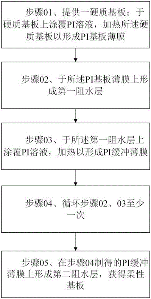
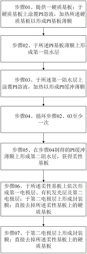
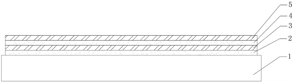
[0050] Step 11. Provide a rigid substrate; apply PI solution on the rigid substrate, and heat the rigid substrate to form a PI substrate film with a thickness of about 0.5 μm;

[0051] Step 12. A first water blocking layer with a thickness of about 1000 nm is formed on the PI substrate film, the first water blocking layer is SiNx, SiO 2 And Al 2 O 3 Any layer or any combination of two or more layers in the inorganic film;

[0052] Step 13. Coat a PI solution on the first water blocking layer and heat to form a PI buffer film with a thickness of about 10 μm;

[0053] Step 14. A second water blocking layer with a thickness of about 200 nm is formed on the PI buffer film; the second water blocking layer is made of SiNx, SiO 2 And Al 2 O 3 Any layer or any combination of two or more layers in the inorganic film;

[0054] Step 15. A first electrode layer (ITO or IZO layer), a...

Embodiment 2

[0057] This embodiment provides a method for manufacturing a flexible OLED device, including the following steps:

[0058] Step 21, providing a rigid substrate; coating PI solution on the rigid substrate, and heating the rigid substrate to form a PI substrate film with a thickness of about 5 μm;

[0059] Step 22: Form a first water blocking layer with a thickness of about 600 nm on the PI substrate film, the first water blocking layer being SiNx, SiO 2 And Al 2 O 3 Any layer or any combination of two or more layers in the inorganic film;

[0060] Step 23: Coating PI solution on the first water blocking layer and heating to form a PI buffer film with a thickness of about 0.5 μm;

[0061] Step 24: Loop the process of steps 22 and 23 5 times;

[0062] Step 25, forming a second water blocking layer with a thickness of about 1000 nm on the PI buffer film obtained in step 24; the second water blocking layer is SiNx, SiO 2 And Al 2 O 3 Any layer or any combination of two or more layers in th...

Embodiment 3

[0066] This embodiment provides a method for manufacturing a flexible OLED device, including the following steps:

[0067] Step 31, providing a rigid substrate; coating PI solution on the rigid substrate, and heating the rigid substrate to form a PI substrate film with a thickness of about 10 μm;

[0068] Step 32: Form a first water blocking layer with a thickness of about 200 nm on the PI substrate film, the first water blocking layer being SiNx, SiO 2 And Al 2 O 3 Any layer or any combination of two or more layers in the inorganic film;

[0069] Step 33: Coating PI solution on the first water blocking layer and heating to form a PI buffer film with a thickness of about 4 μm;

[0070] Step 34: Loop the process of steps 32 and 33 three times;

[0071] Step 35, forming a second water blocking layer with a thickness of about 600 nm on the PI buffer film prepared in step 34; the second water blocking layer is SiNx, SiO 2 And Al 2 O 3 Any layer or any combination of two or more layers in ...


PUM

PropertyMeasurementUnit
thicknessaaaaaaaaaa
thicknessaaaaaaaaaa
thicknessaaaaaaaaaa

Abstract

The invention discloses a flexible substrate manufacturing method which comprises the following steps: 1) providing a hard substrate; coating the hard substrate with PI solution, and heating the hard substrate for a PI substrate film; 2) forming a first water resisting layer on the PI substrate film; 3) coating the first water resisting layer with PI solution and heating the first water resisting layer for a PI buffer film; 4) repeatedly conducting the step 2 and step 3 for at least one more time; and 5) forming a second water resisting layer on the PI buffer film for a flexible substrate. The invention further discloses an OLED device manufacturing method and the applications thereof. According to the invention, PI films and inorganic waterproof layers are alternately designed to form a water resisting layer and then further to form a bendable flexible substrate wherein the PI films serve as both base material films and buffer layer films. With a good winding performance, a good waterproof ability and easy to make, the flexible substrate can be produced in batches.

Description

Technical field [0001] The invention relates to the field of organic photoluminescence, in particular to a method for manufacturing a flexible substrate and a method and application for manufacturing an OLED device. Background technique [0002] Organic Light-Emitting Diodes (OLEDs for short) are self-luminous devices. They are light-weight, ultra-thin, and have high theoretical luminous efficiency. More importantly, they can be made flexible, whether in the field of lighting or display. Will be the future direction of development. Among them, FOLED devices (flexible OLEDs) have the advantages of wide viewing angle and high brightness of ordinary OLED devices. At the same time, because the substrate of FOLED devices is a material with good flexibility, it is lighter, thinner and more compact than ordinary OLED devices using glass substrates. Impact resistance, and the preparation of FOLED devices can adopt a roll-to-roll production method, which can greatly reduce manufacturing ...

Claims


Application Information

Patent Timeline
Patent Type & Authority Applications(China)
IPC IPC(8): H01L51/56
CPCH10K77/111H10K71/00Y02E10/549Y02P70/50
Inventor 赵云张为苍何基强
Owner TRULY SEMICON
Why Eureka
Try Eureka