Semiconductor device

A semiconductor and bipolar transistor technology, applied in the fields of semiconductor devices, semiconductor/solid-state device manufacturing, semiconductor/solid-state device components, etc., can solve problems such as the deterioration of the current amplification rate of bipolar transistors, relieve thermal stress, and suppress thermal resistance. the increasing effect of

Active Publication Date: 2016-08-10
MURATA MFG CO LTD
View PDF5 Cites 4 Cited by
  • Summary
  • Abstract
  • Description
  • Claims
  • Application Information

AI Technical Summary

Problems solved by technology

[0014] For example, in a structure where a bipolar transistor is mounted face-down on a mounting substrate such as a PCB (Printed Circuit Board) substrate as a structure for connecting stud bumps, if the temperature of 150°C or higher is passed through 20 to 50kA / cm 2 current, the current amplification rate of the bipolar transistor deteriorates in a very short time

Method used


Image

  • Semiconductor device
  • Semiconductor device
  • Semiconductor device

Examples


Embodiment approach 1

[0062] Here, a first example of a semiconductor device including a heterojunction bipolar transistor will be described.

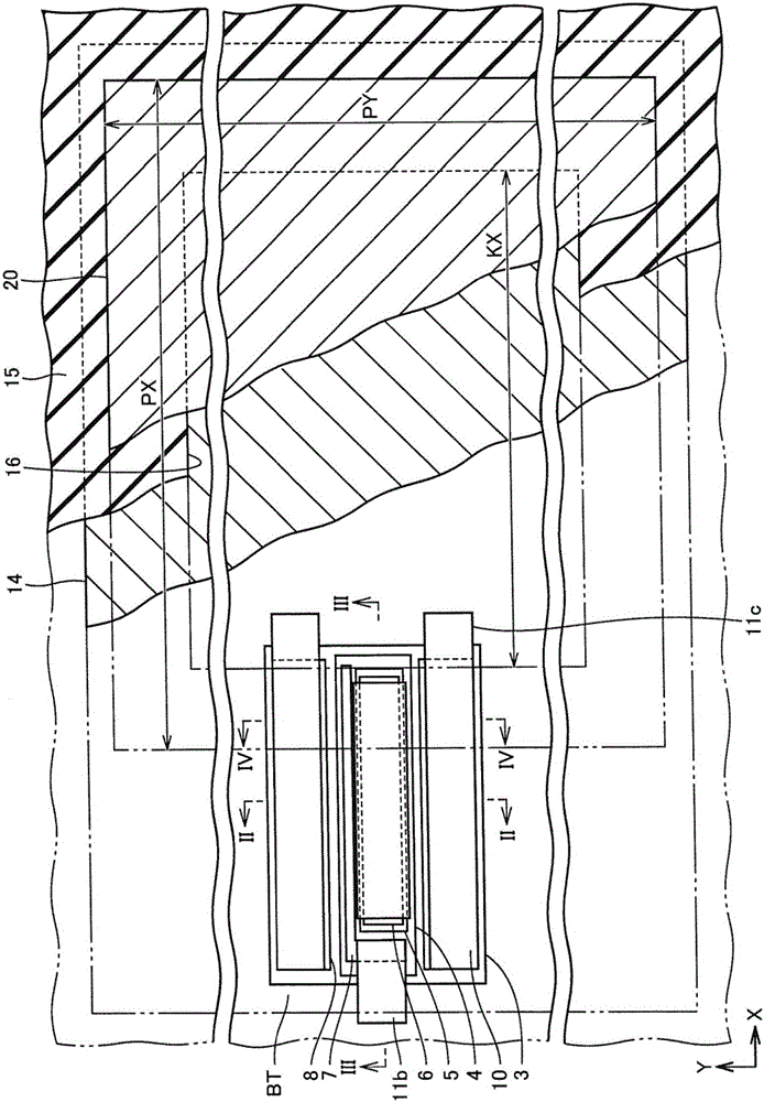
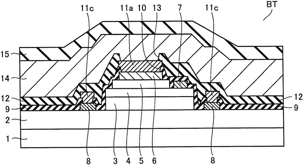
[0063] Such as figure 1 , figure 2 , image 3 as well as Figure 4 As shown, in a semiconductor device equipped with a bipolar transistor BT, the sub-collector layer 2 (n-type GaAs, Si concentration: 5×10 18 cm -3 , film thickness: 0.6 μm) is formed in contact with the surface of the semi-insulating GaAs substrate 1 . Form the collector layer 3 (n-type GaAs, Si concentration: 5×10 15 cm -3 , film thickness: 1.0 μm) is formed in contact with the sub-collector layer 2 . Base layer 4 (p-type GaAs, C concentration: 4×10 19 cm -3 , film thickness: 100 nm) is formed in contact with the collector layer 3 .

[0064] A mesa-shaped emitter layer 5 is formed in contact with the base layer 4 . The emitter layer 5 is stacked sequentially from the side of the base layer 4 with n-type In x Ga 1-x P layer (In composition ratio x=0.5, Si concentration: 3×10 ...

Embodiment approach 2

[0103] Here, as a second example of a semiconductor device including a heterojunction bipolar transistor, a semiconductor device in which rewiring is formed will be described.

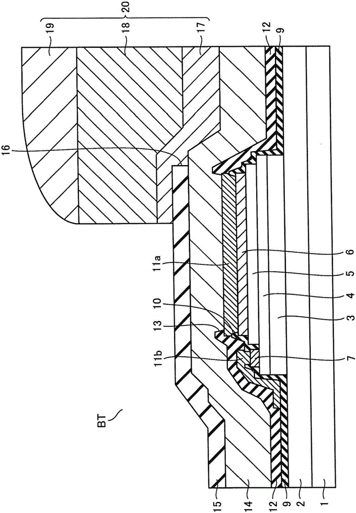
[0104] Such as Figure 24 As shown, for example, a third insulating film 21 (film thickness: 10 μm) composed of a polyimide film or the like is formed to cover the passivation film 15 . A third opening 16 exposing the second wiring 14 is formed in the third insulating film 21 and the passivation film 15 . The third opening 16 is arranged with respect to the emitter layer 5 such that the end of the emitter layer 5 in the longitudinal direction almost coincides with the opening end of the third opening 16 (arrangement C).

[0105] A third wiring 23 (film thickness: 5 μm) made of a copper (Cu) film is formed as a rewiring so as to be in contact with the second wiring 14 exposed at the bottom of the third opening 16 and to be in contact with the opening along the third opening 16. The terminal is in contac...

Embodiment approach 3

[0113] Here, a modification of Embodiment 2 will be described as a third example of a semiconductor device including a heterojunction bipolar transistor.

[0114] Such as Figure 25 As shown, for example, a third insulating film 21 (film thickness: 10 μm) composed of a polyimide film or the like is formed to cover the passivation film 15 . The third opening 16 exposing the second wiring 14 (film thickness: 5 μm) made of a copper (Cu) film is formed in the third insulating film 21 and the passivation film 15 .

[0115] Then, the third wiring 23 as a rewiring is formed in contact with the second wiring 14 exposed at the bottom of the third opening 16 and in contact with the third insulating film 21 arranged along the opening end of the third opening 16 . The third wiring 23 is electrically connected to the emitter layer 5 at a short distance via a portion of the second wiring 14 , a portion of the first wiring 11 a , and the emitter electrode 6 located directly on the emitter l...


PUM

PropertyMeasurementUnit
Film thicknessaaaaaaaaaa

Abstract

Disclosed is a semiconductor device that is provided with a bipolar transistor (BT). In the semiconductor device, a third opening (16) where a pillar bump (20) and second wiring (14) electrically connected to an emitter layer (5) are in contact with each other is disposed by being shifted in the longitudinal direction of the emitter layer (5) from a position corresponding to a portion directly above the emitter layer (5), said third opening (16) being disposed with respect to the emitter layer (5) such that an emitter layer (5) end portion in the longitudinal direction and an opening end of the third opening (16) substantially match.

Description

technical field [0001] The present invention relates to a semiconductor device, and in particular, to a semiconductor device including a heterojunction bipolar transistor. Background technique [0002] In recent years, heterojunction bipolar transistors have been used as transistors constituting power amplifier modules such as mobile terminals. This kind of bipolar transistor is called HBT (Hetero junction Bipolar Transistor: Heterojunction Bipolar Transistor). [0003] Here, an example of a semiconductor device including such a bipolar transistor will be described. Such as Figure 27 , Figure 28 as well as Figure 29 As shown, in the bipolar transistor, the sub-collector layer 102 is formed in contact with the semi-insulating GaAs substrate 101 , and the collector layer 103 is formed in contact with the sub-collector layer 102 . The base layer 104 is formed in contact with the collector layer 103 , and the emitter layer 105 is formed in contact with the base layer 104 ...

Claims


Application Information

Patent Timeline
IPC IPC(8): H01L21/331H01L21/3205H01L21/60H01L21/768H01L23/522H01L29/737
CPCH01L29/41708H01L29/732H01L29/7371H01L2224/05569H01L24/02H01L24/03H01L24/05H01L24/16H01L2224/02331H01L2224/0235H01L2224/0239H01L2224/0401H01L2224/05022H01L2224/05147H01L2224/05558H01L2224/05559H01L2224/05666H01L2224/13013H01L2224/13022H01L2224/13024H01L2224/131H01L2224/13111H01L2224/13147H01L2224/16227H01L2924/13055H01L2224/03912H01L2224/05572H01L29/66272H01L29/0692H01L29/0817H01L29/66242H01L29/66318H01L29/205H01L24/13H01L2924/01079H01L2924/00012H01L2924/00014H01L2924/01029H01L2924/014H01L29/737H01L29/66234H01L29/6631H01L29/7375H01L29/7378H01L2224/02372H01L2224/02373H01L2224/05024H01L2224/05166H01L2224/13026H01L2224/13563H01L2224/13611H01L2224/16235H01L2924/10329H01L2924/10337H01L2924/10338H01L2924/13051H01L2924/351H01L24/11H01L29/20H01L2224/024H01L2224/1134H01L2224/13083H01L2224/13155H01L2224/16225H01L2924/07025H01L2924/1423
Inventor 梅本康成德田大辅西明恒和德矢浩章
Owner MURATA MFG CO LTD
Why Eureka
Try Eureka