A layer-changing wiring method, device and integrated circuit system

An integrated circuit and first-line technology, applied in printed circuit, printed circuit manufacturing, printed circuit components, etc., can solve problems such as poor continuity of line signal impedance, high density of VIA holes, and large interference

Active Publication Date: 2019-01-11
LANGCHAO ELECTRONIC INFORMATION IND CO LTD
View PDF3 Cites 0 Cited by
  • Summary
  • Abstract
  • Description
  • Claims
  • Application Information

AI Technical Summary

Problems solved by technology

When simulating according to the existing layer-changing wiring method, it is found that because the PIN pin density of BGA components is relatively high, and VIA holes are drilled on the PIN pins, the density of VIA holes is also large, and the interference between lines is relatively large. The impedance continuity of the line signal at the VIA hole is poor

Method used


Image

  • A layer-changing wiring method, device and integrated circuit system
  • A layer-changing wiring method, device and integrated circuit system
  • A layer-changing wiring method, device and integrated circuit system

Examples


Embodiment Construction

[0048] In order to make the purpose, technical solutions and advantages of the embodiments of the present invention clearer, the technical solutions in the embodiments of the present invention will be clearly and completely described below in conjunction with the drawings in the embodiments of the present invention. Obviously, the described embodiments It is a part of the embodiments of the present invention, but not all of them. Based on the embodiments of the present invention, all other embodiments obtained by those of ordinary skill in the art without creative work belong to the protection of the present invention. scope.

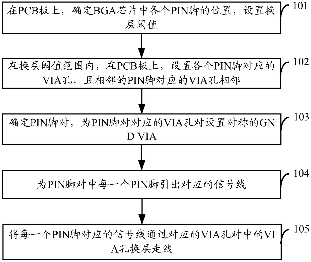
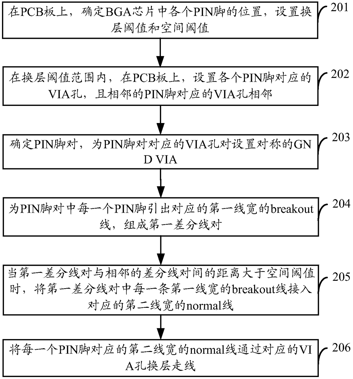
[0049] Such as figure 1 As shown, the embodiment of the present invention provides a layer-changing routing method, which may include the following steps:

[0050] Step 101: on the PCB board, determine the position of each PIN pin in the BGA chip, and set the layer change threshold;

[0051] Step 102: within the layer change threshold range, on the PC...


PUM


Abstract

The invention provides a layer-changing wiring method, device and integrated circuit system. The method determines the position of each PIN pin in the BGA chip on the PCB board, sets the layer-changing threshold, and within the range of the layer-changing threshold, the PCB On the board, set the VIA holes corresponding to each PIN pin, and the VIA holes corresponding to the PIN pins are adjacent; determine the PIN pin pair, and set a symmetrical GND VIA for the VIA hole pair corresponding to the PIN pin pair; lead out each PIN pin in the PIN pin pair Corresponding signal lines; route the signal lines corresponding to each PIN through the VIA holes in the corresponding VIA hole pairs. The scheme provided by the invention effectively improves the impedance continuity of the line signal at the VIA hole.

Description

technical field [0001] The invention relates to the technical field of communications, in particular to a layer-changing routing method, device and integrated circuit system. Background technique [0002] With the miniaturization trend of electronic products, the size of the PCB board is getting smaller and smaller, and the BGA components on the PCB board often need to change layers to achieve communication. [0003] At present, the method of layer-changing routing is mainly to punch VIA holes on the PIN pins before BGA component packaging, and hollow out the outer edge of the VIA holes, so that the lines can be changed through the VIA holes. When simulating according to the existing layer-changing routing method, it is found that because the PIN pin density of BGA components is relatively high, and VIA holes are drilled on the PIN pins, the density of VIA holes is also relatively large, and the interference between lines is relatively large. The impedance continuity of the...

Claims


Application Information

Patent Timeline
Patent Type & Authority Patents(China)
IPC IPC(8): H05K1/11H05K3/40
CPCH05K1/115H05K3/4038
Inventor 孙龙张春丽
Owner LANGCHAO ELECTRONIC INFORMATION IND CO LTD
Why Eureka
Try Eureka