An array substrate and a liquid crystal display panel including the same

An array substrate and array technology, applied in the field of liquid crystal display panels, can solve problems such as small storage capacitance, afterimages, and flickering in the display process, and achieve the effects of improving flickering, increasing capacity, and improving display effects

Active Publication Date: 2019-05-24
SHANGHAI AVIC OPTOELECTRONICS +1
View PDF8 Cites 0 Cited by
  • Summary
  • Abstract
  • Description
  • Claims
  • Application Information

AI Technical Summary

Problems solved by technology

[0004] In the existing liquid crystal display panel with transverse electric field (for example, IPS, In-Plane Switching), due to the small storage capacitance in each pixel, problems such as flickering and afterimage are prone to occur during the display process

Method used


Image

  • An array substrate and a liquid crystal display panel including the same
  • An array substrate and a liquid crystal display panel including the same
  • An array substrate and a liquid crystal display panel including the same

Examples


Embodiment Construction

[0020] The present invention will be further described in detail below with reference to the drawings and embodiments. It can be understood that the specific embodiments described here are only used to explain the related invention, but not to limit the invention. In addition, it should be noted that, for ease of description, only the parts related to the invention are shown in the drawings.

[0021] It should be noted that the embodiments of the present invention and the features in the embodiments can be combined with each other if there is no conflict. Hereinafter, the present invention will be described in detail with reference to the drawings and in conjunction with the embodiments.

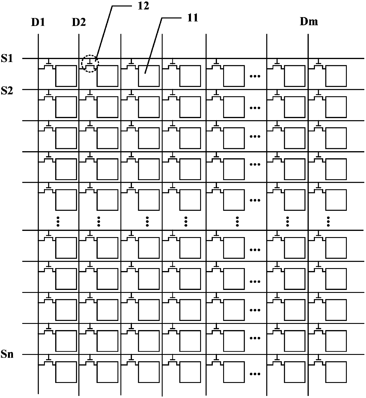
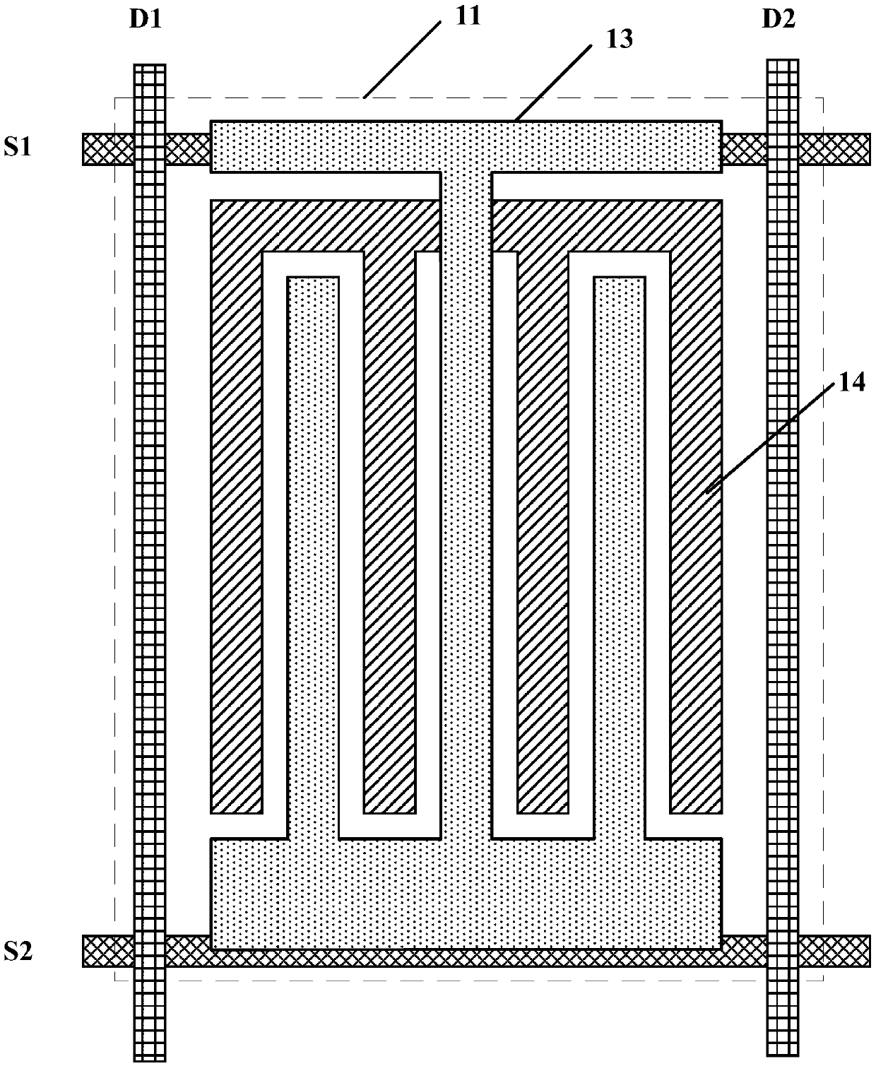
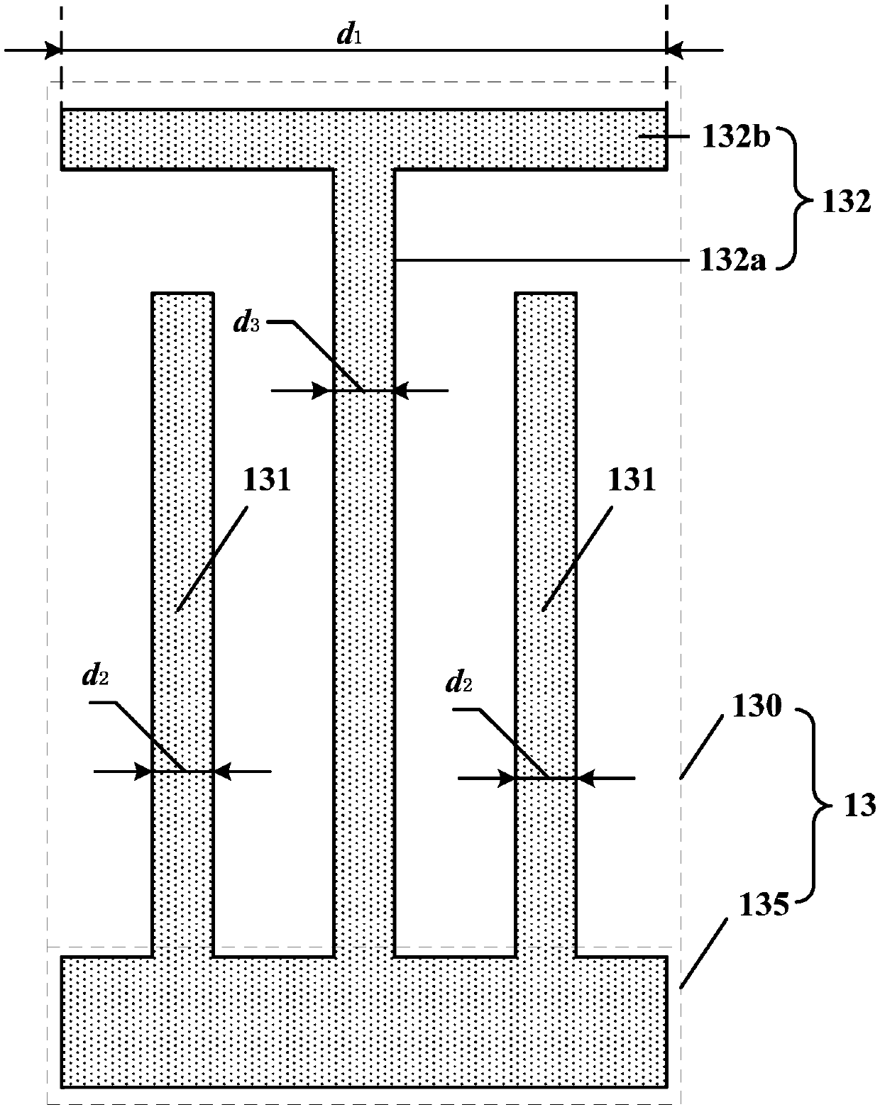
[0022] In addition, it should be noted that in the following embodiments and corresponding drawings, the reference signs S1 and S2 represent two adjacent scan lines, and the reference signs D1 and D2 represent two adjacent data lines.

[0023] See Figure 1 to Figure 4 ,among them, figure 1 Is a ...


PUM


Abstract

The invention discloses an array substrate and a liquid crystal display panel comprising the array substrate. Each display pixel of the array substrate comprises a pixel electrode and a public electrode for forming a transverse electric field together with the pixel electrode inside. According to the scheme of the invention, the pixel electrodes are provided with electrode portions overlapped with scanning lines, so that the capacitance of storage capacitors inside the display pixels is increased, thereby solving the problems of flickering, residual images and the like during displaying, and improving the display effect.

Description

Technical field [0001] The present invention relates to the field of display technology, and in particular to an array substrate and a liquid crystal display panel including the same. Background technique [0002] A liquid crystal display panel usually includes an array substrate, a color filter substrate disposed opposite to the array substrate, and a liquid crystal layer located between the array substrate and the color filter substrate. The array substrate is provided with a thin film transistor array, a pixel electrode array and a common electrode. Each thin film transistor of the thin film transistor array applies a data signal to each pixel electrode in the pixel electrode array, and applies a common voltage to the common electrode through a common voltage signal line, so that an electric field is formed between the pixel electrode and the common electrode, and the liquid crystal molecules in the liquid crystal layer It is deflected under the action of electric field to re...

Claims


Application Information

Patent Timeline
Patent Type & Authority Patents(China)
IPC IPC(8): G02F1/1343G02F1/1362
CPCG02F1/134363G02F1/136213
Inventor 金慧俊
Owner SHANGHAI AVIC OPTOELECTRONICS
Why Eureka
Try Eureka