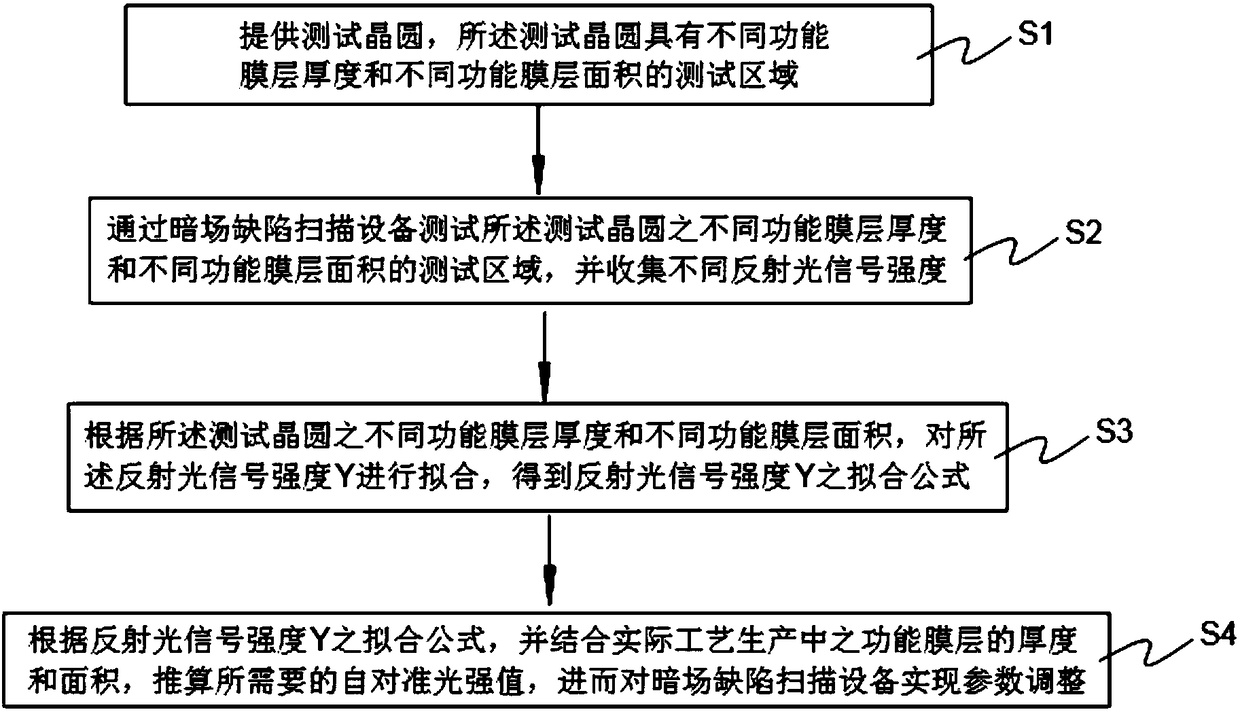
A correction method for self-alignment process window of dark field defect detection equipment
A self-alignment process and defect detection technology, applied in semiconductor/solid-state device testing/measurement, electrical components, circuits, etc., can solve problems such as self-alignment, failure, and no clear method, and avoid self-alignment Quasi-failure effect
- Summary
- Abstract
- Description
- Claims
- Application Information
AI Technical Summary
Problems solved by technology
Method used
Image
Examples
Embodiment Construction
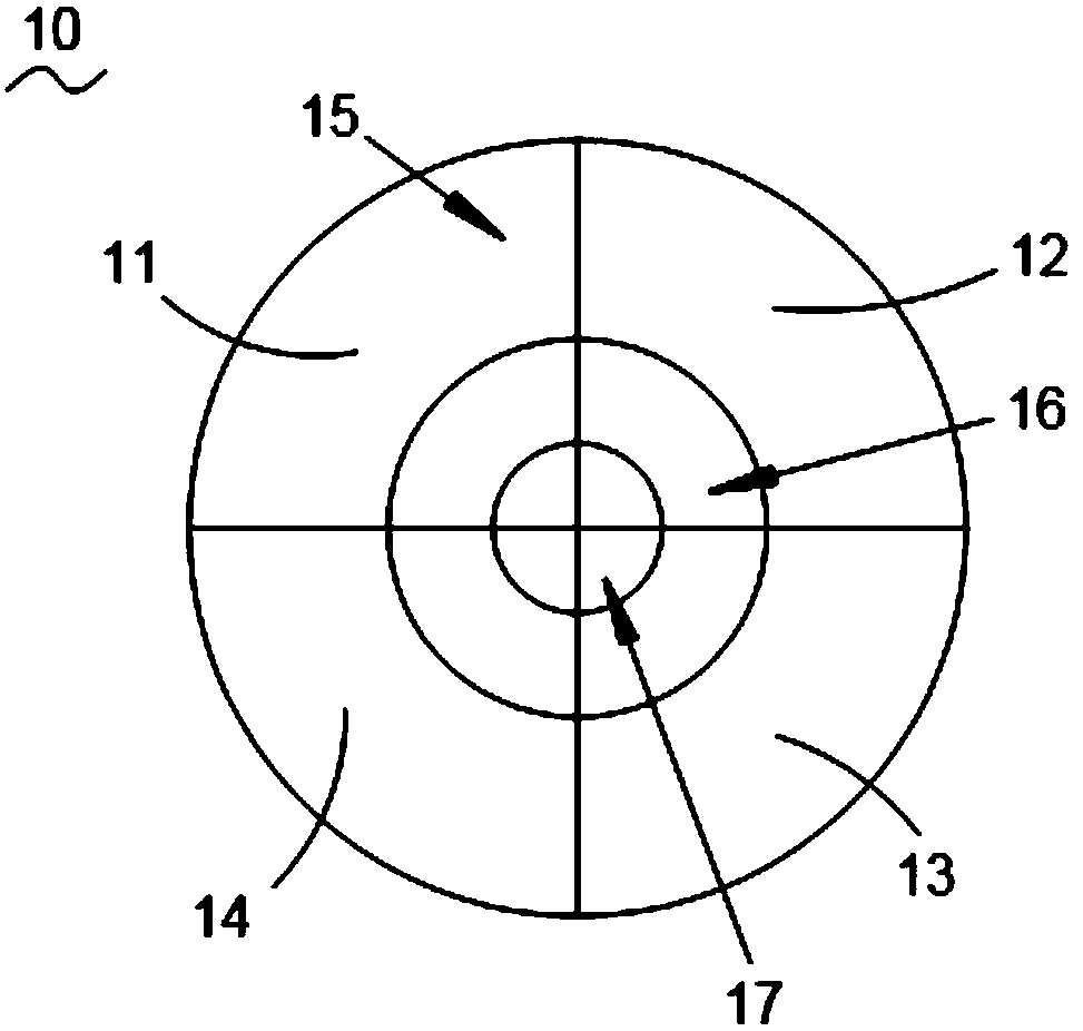
[0025] In order to illustrate the technical content, structural features, achieved goals and effects of the present invention in detail, the following will be described in detail in conjunction with the embodiments and accompanying drawings.
[0026] The dark field defect detection equipment needs to perform real-time self-alignment correction during the scanning process to adjust the distance between the wafer and the light source to achieve the best self-alignment effect. With the development of integrated circuit technology and the scaling down of key dimensions, as well as the increase in the complexity of semiconductor manufacturing, the materials and thickness of the films that need to be filled also have more diverse changes.
[0027] The self-alignment system of dark-field defect scanning equipment usually uses a single light source for self-alignment calibration for all thin-film materials, and the following defects will obviously appear: for particularly dark thin-fil...
PUM
 Abstract
Description
Claims
Application Information


