Electronic component detection method and device

An electronic component and detection method technology, which is applied in the field of electronic component detection and device, can solve the problems of high cost, time-consuming assembly cost, complexity, etc., and achieve the effects of being less prone to failure, saving costs, and simplifying space.

Active Publication Date: 2016-09-28
ALL RING TECH CO LTD
View PDF7 Cites 8 Cited by
  • Summary
  • Abstract
  • Description
  • Claims
  • Application Information

AI Technical Summary

Problems solved by technology

[0005] In the prior art, optical fiber sensing elements respectively located above and below the loading slot of the turntable of the sorting mechanism are used. When the transmitting end of the optical fiber sensing element below sends out a light source signal, the receiving end of the optical fiber sensing element above receives the light source signal. The light source must be introduced into the detection amplifier. Due to the large size and high cost of the detection amplifier, each optical fiber sensing element must be connected to the detection amplifier. The turntable of a general sorting mechanism usually has more than 20 loading slots to transport electronic components. There are more than 20 wires of optical fiber sensing elements above the turntable of the sorting mechanism. In addition, the optical fiber sensing elements located above the turntable as the receiving end must correspond to each slot on the turntable in a vertical direction, so each slot of the turntable The upper part must be set according to the corresponding position of each optical fiber sensing element, and then respectively set the fixing components to fix each optical fiber sensing element so that it can correspond to each slot on the turntable in the vertical direction, then more than 20 optical fiber sensing elements The wires and the arrangement of more than 20 sets of fixed components make the top of the turntable of the sorting mechanism extremely complicated and prone to confusion and failure, and the assembly cost is time-consuming, labor-intensive, and costly!

Method used


Image

  • Electronic component detection method and device
  • Electronic component detection method and device
  • Electronic component detection method and device

Examples


Embodiment Construction

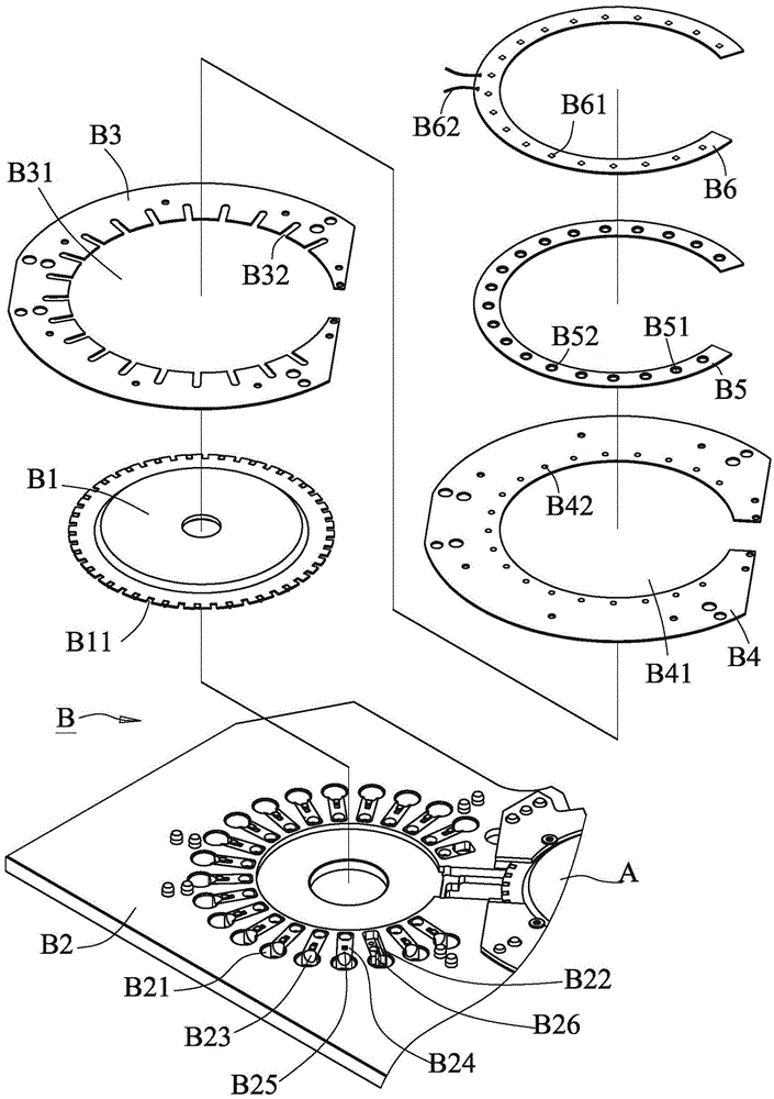
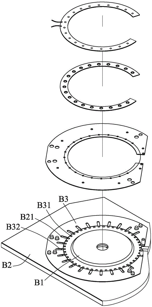
[0039] see figure 1 , 2 , the electronic component testing method and device of the embodiment of the present invention uses the test plate A as shown in the figure to carry the test component intermittently in the rotating flow path. After going through the procedures of multiple testing stations, according to the detected physical characteristics, It is illustrated by the classification mechanism B of the turntable B1 similar to the aforementioned measuring disk A, which has a circumferential arrangement of equally spaced concave loading slots B11, wherein:

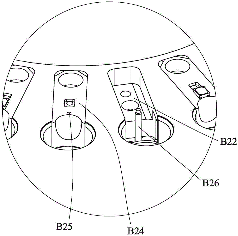
[0040] The sorting mechanism B is provided with a plurality of discharge outlets B21 which are respectively connected to discharge pipes (not shown in the figure) in a ring row on the machine table B2; Groove B22 is used to accommodate the block B24 that forms a part of the arc concave part B23 of the discharge port; each block B24 is provided with a detection hole B25 near the arc concave part B23, which is located be...


PUM


Abstract

The invention provides an electronic component detection method and a device. The electronic component detection method enables a detected element to be transported through a rotation flow path in an intermittent manner and subjects the element to a sorting mechanism of a turntable concavely provided with loading slots at equal intervals along the circumferential direction thereof. The sorting mechanism is provided with a discharge outlet. a detected element conveying flow path, between the loading slots and the discharge outlet, is provided with first sensing elements served as receiving terminals to receive a light source signal emitted by an LED, and second sensing elements served as transmitting terminals to send out the light source signal of the LED. The plurality of second sensing elements and the circuits thereof are loaded on a carrier. Each circuit is connected with an external other control circuit interface through the same group of conducting wires, so that whether the detected element is discharged out of the loading slots to the discharge outlet or not can be detected. Therefore, mechanisms above the turntable are concise, and the cost is reduced.

Description

technical field [0001] The present invention relates to a detection method and device, especially an electronic component detection method and device for detecting electronic components discharged from a sorting mechanism to a sorting tube during the sorting and sorting process of electronic components. Background technique [0002] Due to the different physical characteristics of general electronic components, they often need to be packaged or classified through testing and sorting procedures. Due to the miniaturization and large-scale properties of electronic components, the devices used for testing and sorting must provide rapid and accurate The transportation of these detected and sorted electronic components such as passive components or LED light-emitting diodes. [0003] When testing in the prior art, a measuring disc that can be used for intermittent rotation is often used, and concave loading slots with equal intervals are arranged around the circumference of the te...

Claims


Application Information

Patent Timeline
Patent Type & Authority Applications(China)
IPC IPC(8): B07C5/00
CPCB07C5/00
Inventor 纪建兆
Owner ALL RING TECH CO LTD
Why Eureka
Try Eureka