Display device and its liquid crystal display panel, liquid crystal display module

A liquid crystal display module, array substrate technology, applied in the direction of instruments, nonlinear optics, optics, etc., to achieve the effect of increasing standing stability, increasing the accuracy of the group, and avoiding the effect of slipping off the contact point of the electrode signal test

Active Publication Date: 2019-05-07
WUHAN CHINA STAR OPTOELECTRONICS TECH CO LTD
View PDF8 Cites 0 Cited by
  • Summary
  • Abstract
  • Description
  • Claims
  • Application Information

AI Technical Summary

Problems solved by technology

[0004] An embodiment of the present invention provides a liquid crystal display device, its liquid crystal display panel, and a liquid crystal display module to solve the technical contradiction between high aperture ratio and high support stability in the design process of spacers for liquid crystal display panels in the prior art question

Method used


Image

  • Display device and its liquid crystal display panel, liquid crystal display module
  • Display device and its liquid crystal display panel, liquid crystal display module
  • Display device and its liquid crystal display panel, liquid crystal display module

Examples


Embodiment Construction

[0027] The present invention will be described in further detail below in conjunction with the accompanying drawings and embodiments. especially

[0028] It should be noted that the following examples are only used to illustrate the present invention, but not to limit the scope of the present invention. Likewise, the following embodiments are only some but not all embodiments of the present invention, and all other embodiments obtained by persons of ordinary skill in the art without creative efforts fall within the protection scope of the present invention.

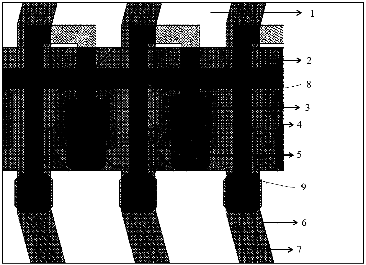
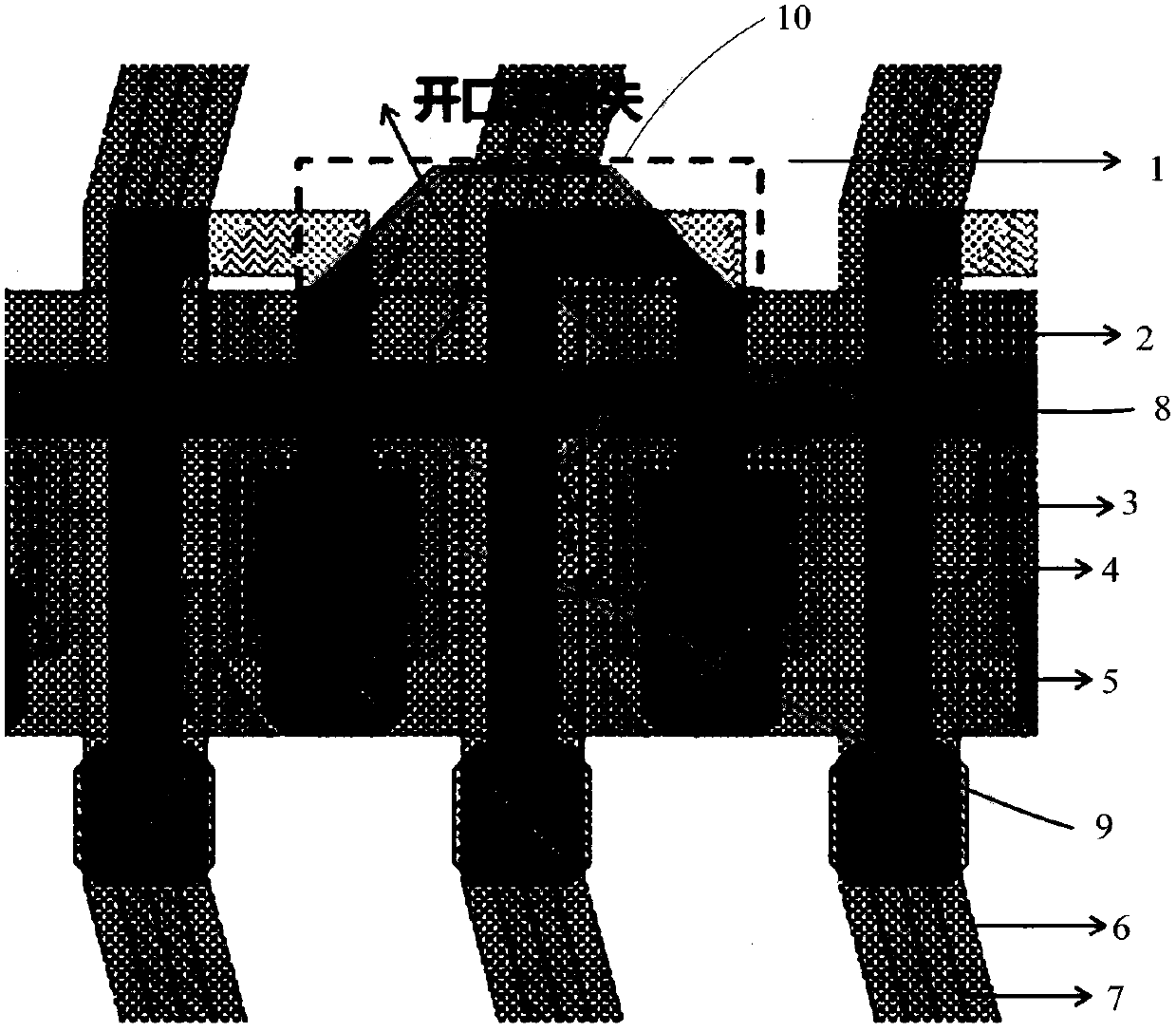
[0029] Please also refer to Image 6 with Figure 7 , Image 6 It is a schematic diagram of the structure before the array substrate and the color filter substrate are assembled in the liquid crystal display module of the present invention, Figure 7 It is a schematic diagram of the structure after the array substrate and the color filter substrate are assembled in the liquid crystal display module of the present inve...


PUM


Abstract

The invention provides a liquid crystal display device and a liquid crystal display panel thereof and a liquid crystal display module. The liquid crystal display module comprises a color film substrate, an array substrate and multiple columnar spacers arranged between the color film substrate and the array substrate; each columnar spacer is provided with a taper, the big end of each taper is connected with the color film substrate, and the small end of each taper abuts against the array substrate; the length of the end face of the small end of each columnar spacer which abuts against the array substrate is larger than the distance between adjacent sub-pixel connecting through holes formed in an array substrate photoresist layer. According to the liquid crystal display module, due to the fact that the end faces of the small end of the columnar spacers are designed to be shaped like long stripes or rhombuses or the like, after the array substrate and the color film substrate are combined in a paired mode, the columnar spacers can be packed into the adjacent sub-pixel connecting through holes, the columnar spacers can be in occluding contact with a protrusion of an upper insulating layer of an electrode signal test contact point, the standing stability of the columnar spacers is improved, and therefore the risk that display is poor due to the fact that a PS slides down the electrode signal test contact point is reduced.

Description

technical field [0001] The invention relates to the technical field of liquid crystal display devices, in particular to a liquid crystal display device, a liquid crystal display panel, and a liquid crystal display module. Background technique [0002] Existing small-size LCDs generally use double-column height PS (Post Spacer, columnar spacer), that is, the PS on the CF side has two column heights, and the main column PS (Main PS) is higher but less distributed. For LCD It plays the role of the thickness of the main support box; the auxiliary column PS (Sub PS) is low but densely distributed, which is used to increase the compressive capacity of the panel. The height and standing position of the PS will also affect the liquid crystal droplet dosage of the LCD in the Cell segment. [0003] With the market demand of LCD panels, high aperture ratio and high PPI (Pixels Per Inch also called pixel density) have become important goals of panel (substrate) design. As the PPI gets...

Claims


Application Information

Patent Timeline
Patent Type & Authority Patents(China)
IPC IPC(8): G02F1/1339
CPCG02F1/13394
Inventor 张启沛陈彩琴
Owner WUHAN CHINA STAR OPTOELECTRONICS TECH CO LTD
Why Eureka
Try Eureka