

An auxiliary manual wafer bonding device
A wafer bonding and wafer technology, applied in the manufacture of electrical components, electrical solid devices, semiconductor/solid devices, etc., can solve problems such as wafer surface pollution, affecting bonding quality, bonding interface defects, etc., to reduce The effect of pollutants introduced by the surrounding environment and human operation, shortening the manual operation time, and improving the effect
- Summary
- Abstract
- Description
- Claims
- Application Information
AI Technical Summary
Problems solved by technology
Method used
Image

Examples
specific Embodiment approach 1
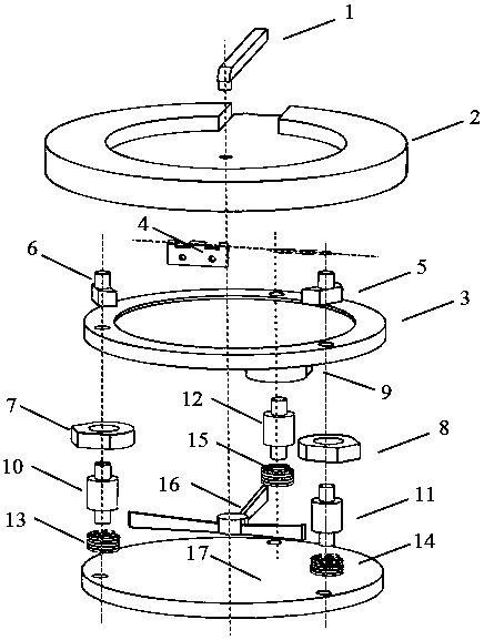
[0025] Specific implementation mode one: combine Figure 1~Figure 3 Describe this embodiment, the auxiliary wafer bonding device in this embodiment consists of a long right-angle elbow joint 1, a wafer slot A 2, a wafer slot B 3, a fixed angle (180°) hinge 4, and a buffer block A 5 , buffer block B6, linear bearing A 7, linear bearing B 8, linear bearing C 9, linear optical axis A 10, linear optical axis B 11, linear optical axis C 12, spring A 13, spring B 14, spring C 15, Linear bearing connector 16 and base 17 constitute, wherein:
[0026] The central position of the wafer slot A 2 is provided with a central through hole with a diameter of 4 mm so as to be connected to the shorter end of the long right-angle elbow joint 1; the upper surface of the wafer slot A 2 is in the shape of an "Ω" Groove-shaped, and its depth is slightly higher than the height of the longer end of the long right-angle elbow joint 1 by 0.5-1.0 mm; the lower surface of the wafer slot A 2 is provided w...
specific Embodiment approach 2
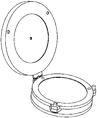
[0034] Specific implementation mode two: combination Figure 4~Figure 7 To illustrate this embodiment, a 3-inch silicon wafer passes through an RCA solution (NH 4 OH:H 2 o 2 :H 2 O = 0.01~0.25:1:5) and after wet cleaning with deionized water, if Figure 4 As shown, use tweezers to pick up the wafers and place them in wafer slot A and wafer slot B respectively, and start the vacuum generating device connected to the long right-angle elbow joint to suck the wafer in wafer slot A to prevent Wafers fall off during the transfer of wafer tank A.
[0035] After the wafers are placed in wafer slot A and wafer slot B, use a nitrogen gun to dry up the liquid adsorbed on the wafer surface, such as Figure 5 As shown, since the periphery of the wafer is slightly higher than the edge of wafer slot A and wafer slot B, and there are no fingers blocking the surrounding area, the problem of wafer surface contamination due to stagnation of liquid will not be caused.
[0036] After the waf...
specific Embodiment approach 3
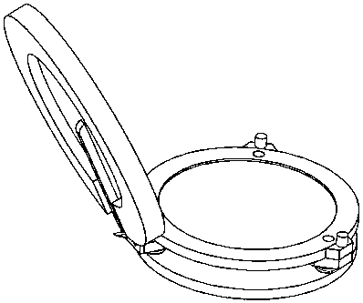
[0037] Specific implementation mode three: combination Figure 8To illustrate the embodiment of the present invention, the device for assisting wafer bonding is not only applicable to accomplish the above steps, but also applicable to dry surface treatment using ultraviolet light irradiation, and then performing wafer bonding.
[0038] After drying the wafer, use an ultraviolet light source (such as wavelength 172 nm, light intensity 10 mW / cm 2 ) to irradiate the surfaces of two wafers for 20 minutes at the same time, to remove the organic pollution (such as dust particles, etc.) attached to the surface, and to improve the hydrophilicity of the surface. Since ultraviolet light will be absorbed by oxygen in the air to a large extent, when the wafer is irradiated with ultraviolet light, the distance between the ultraviolet tube light source and the surface of the wafer to be processed should be strictly controlled (<5 mm ). After the ultraviolet light irradiation is completed,...
PUM
 Abstract
Description
Claims
Application Information