

Wafer vacuum bonding machine and bonding method
A vacuum bonding machine and wafer technology, applied in the field of microelectronics, can solve the problems of complex structure and high cost
- Summary
- Abstract
- Description
- Claims
- Application Information
AI Technical Summary
Problems solved by technology
Method used
Image

Examples
Embodiment
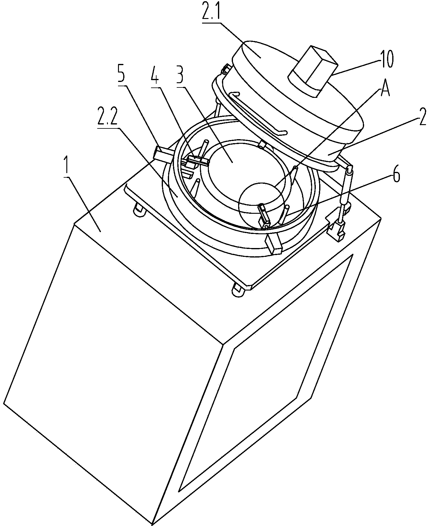
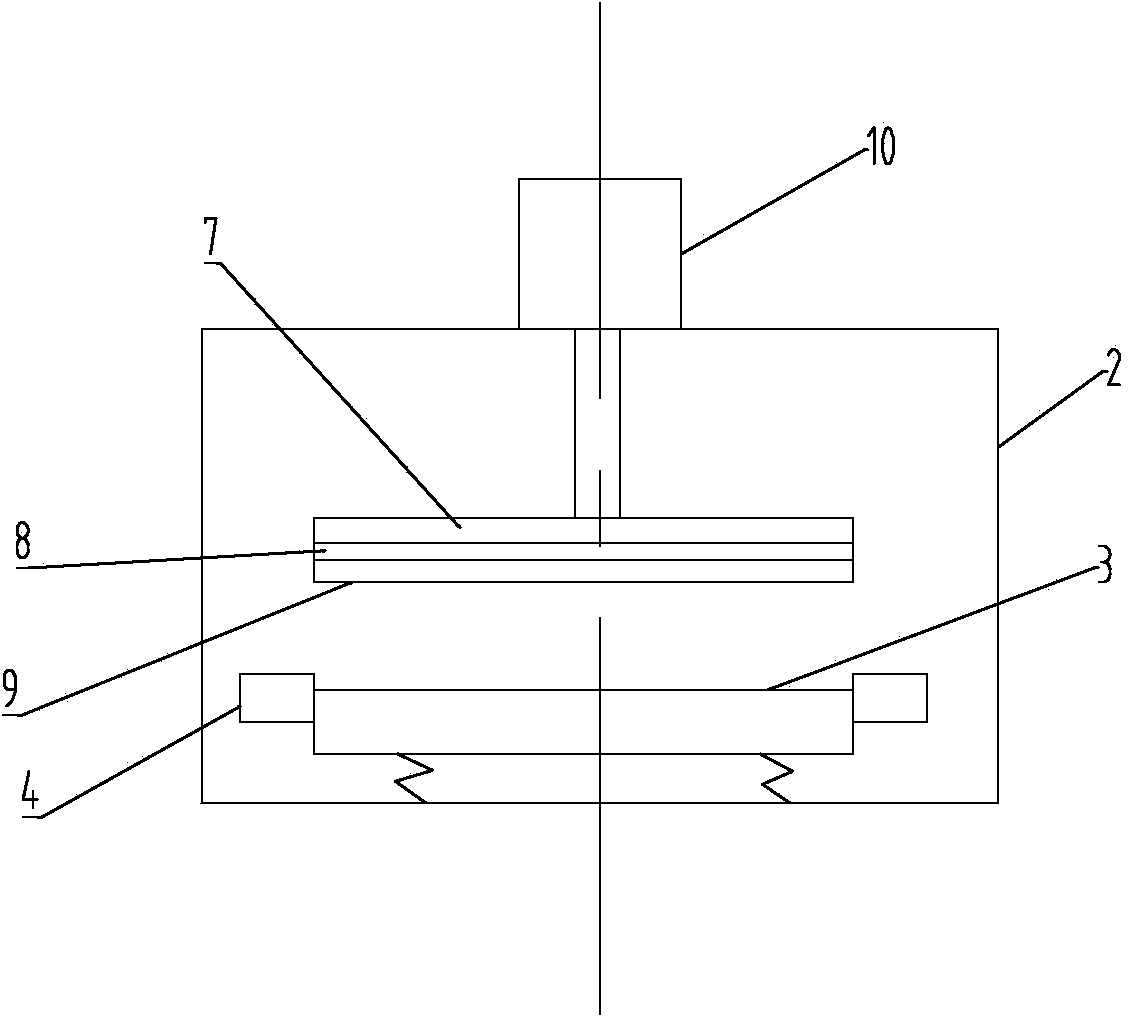
[0048] Embodiment: In this embodiment, two wafers with a thickness of more than 0.3 mm and a diameter of 200 mm are used, and the bonding steps are as follows:
[0049] S1. Put the first wafer coated with bonding glue on the tray;
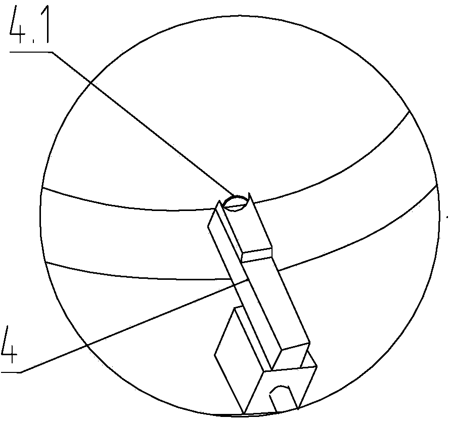
[0050] S2. Control multiple positioning blocks to advance toward the pallet through the cylinder, and position the first wafer at the center;
[0051] S3. Place the second wafer on the positioning block support, then close the cover to close the press, and evacuate;
[0052] S4, when the vacuum degree reaches 10 Pa, control multiple positioning blocks to retreat, and the second wafer falls from the positioning block support to the first wafer;
[0053] S5, the multiple positioning blocks are controlled by the cylinder to advance toward the tray again, and the two wafers are positioned to completely overlap the edges of the two wafers;
[0054] S6. The pressing plate is controlled downward by the press, so that the first wafer and the second wafer...
PUM
 Abstract
Description
Claims
Application Information