Method for packaging wafer level glass micro-cavity of light-emitting diode (LED)

A technology of light-emitting diodes and packaging methods, which is applied in the direction of electrical components, electric solid devices, circuits, etc., can solve the problems of poor moisture resistance of organic matter, poor light transmission of lenses, and low efficiency of phosphor powder, so as to achieve anti-aging and simple process Reliable, high light output effect

Active Publication Date: 2011-06-29
SOUTHEAST UNIV
View PDF5 Cites 13 Cited by
  • Summary
  • Abstract
  • Description
  • Claims
  • Application Information

AI Technical Summary

Problems solved by technology

Nowadays, transparent organic adhesives such as epoxy resin are widely used in the preparation of light-emitting diode (LED) lenses, but the lenses made of organic adhesives have poor light transmission and unstable properties. When heated, they will change color after working for a certain period of time. , the light transmission performance becomes poor, and the moisture resistance of organic matter is poor
[0004] At present, the phosphor coating of light-emitting diodes (LEDs) is mostly applied by dispensing glue (silica gel mixed with phosphor) on the chip, so that the efficiency of phosphor coating is very low; and the packaging of the chip also uses Dispensing and curing method, package by package
This method of monolithic packaging is very inefficient, so if wafer-level phosphor coating and packaging can be performed, efficiency will be greatly improved and costs will be reduced

Method used


Image

  • Method for packaging wafer level glass micro-cavity of light-emitting diode (LED)
  • Method for packaging wafer level glass micro-cavity of light-emitting diode (LED)
  • Method for packaging wafer level glass micro-cavity of light-emitting diode (LED)

Examples


Embodiment 1

[0034] A wafer-level glass microcavity packaging method for light-emitting diodes, comprising the following steps:

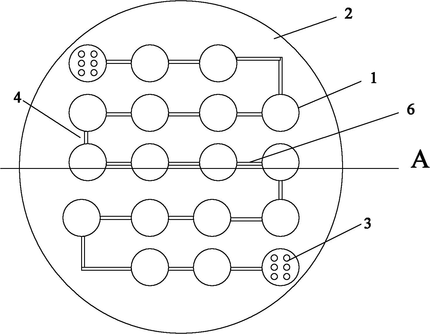
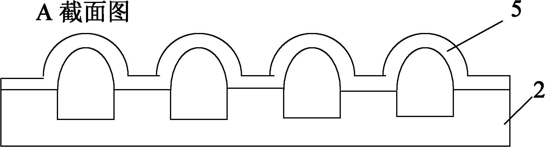
[0035] The first step is to etch specific microgrooves and microchannel patterns on Si wafers (such as 4-inch wafers) using Si micromachining technology. The microgrooves are connected to the microchannels, and the microgrooves can be square or circular. The size ratio of pattern, microgroove and microchannel is adjusted according to the preparation requirements, and an appropriate amount of thermal air release agent is placed in the microgroove; in the second step, the above Si wafer with pattern and thermal air release agent is combined with Pyrex7740 borosilicate The glass wafers are anodically bonded in the air or in vacuum to seal the above-mentioned microgrooves and micro-flow channels to form a sealed cavity; the third step is to heat the above-mentioned bonded wafers to 820°C~950°C in the air ℃, and keep it warm for 0.5~10min, the positive pressure forme...

Embodiment 2

[0038] A wafer-level glass microcavity packaging method for light-emitting diodes, comprising the following steps:

[0039] The first step is to use the Si micromachining process to etch the wet pattern corresponding to the packaged LED array on the Si wafer (such as a 4-inch wafer): a micro-groove array (80um in depth), and the micro-grooves are separated by micro-grooves. The flow channels are connected, the microgroove is circular, and an appropriate amount of heat release agent calcium carbonate is placed in the microgroove.

[0040] In the second step, the above-mentioned Si wafer with the pattern and thermal air release agent is anodically bonded to the Pyrex7740 glass wafer in vacuum, so that the Pyrex7740 glass forms a sealed cavity with the above-mentioned microgrooves and micro-channels.

[0041] The third step is to heat the above-bonded wafers to 880°C in the air and keep it warm for 10 minutes. The heat release agent calcium carbonate will generate positive pressu...

Embodiment 3

[0048] A method for manufacturing a wafer-level glass microcavity for LED packaging, comprising the following steps:

[0049] The first step is to oxidize a 5000A oxide layer on a single-sided polished silicon wafer by a combination of dry and wet oxygen, spin-coat AZ P4620 photoresist on the polished surface, expose and develop to remove the photoresist that needs to be etched on the surface of the microgroove. Use Si micromachining technology to etch shallow grooves on Si wafers (such as 4-inch wafers). The silicon wafers used can be silicon wafers with a standard thickness, such as 500 micron thick silicon wafers. The shallow grooves are etched by TMAH wet etching. Etching, heating in a water bath at 90°C for 2 to 2.5 hours, the etching depth is 80 to 120, this depth can be relatively easy to build a thermal release agent, and can provide a certain space between the thermal release agent and the wafer to avoid contact with the glass The contact produces pollution, and the p...


PUM


Abstract

The invention discloses a method for packaging a wafer level glass micro-cavity of a light-emitting diode (LED), and the method comprises the following steps: (1) etching a micro-slot array corresponding to the pattern of a packaged LED array on a silicon wafer, wherein the micro-slots are communicated through a micro-channel, and a proper amount of heat gas releasing agent is arranged inside the micro-slots; (2) forming a closed cavity; (3) heating the bonded wafer in the air to form a spherical glass micro-cavity and a cylindrical glass micro-channel connected with the spherical glass micro-cavity, cooling to room temperature, annealing, and removing silicon to obtain a wafer level glass micro-cavity; (4) sputtering a metal layer on the silicon wafer, and preparing a metal lead through photolithography, so as to obtain a lead substrate, wherein the position of the metal lead corresponds to the position of the micro-channel of the glass micro-cavity; (5) mounting an LED chip on the lead substrate, and leading; (6) bonding the wafer level glass micro-cavity with the substrate to form a bonded wafer; and (7) filling the gap between the LED chip and the wafer level glass micro-cavity with silicone through the glass micro-channel. According to the invention, the light emitting efficiency is high, and a packaged glass lens realizes beam collimation.

Description

technical field [0001] The invention relates to a MEMS (micro-electro-mechanical system) packaging technology, in particular to a wafer-level glass microcavity packaging method for light-emitting diodes. Background technique [0002] The development of white light-emitting diode (LED) technology has brought us into the fourth generation of lighting. White light-emitting diode (LED) lighting will surely replace today's lighting technology due to its advantages of low energy consumption and environmental protection. For lighting purposes, high-power white light-emitting diodes (LEDs) have been widely concerned by scientific research and enterprises. In order to generate sufficient light intensity, the working current of light-emitting diodes (LEDs) must be as large as possible, and the large working current is required for the packaging of light-emitting diodes (LEDs). The heat dissipation problem of the system has brought serious challenges. Therefore, by designing the opti...

Claims


Application Information

Patent Timeline
Patent Type & Authority Applications(China)
IPC IPC(8): H01L33/00H01L25/075H01L33/48H01L33/58H01L33/62H01L33/64
CPCH01L2224/48091H01L2924/10253H01L24/45H01L2224/45144H01L2224/85207H01L2224/45H01L2924/12041H01L2924/1461
Inventor 尚金堂徐超陈波寅张迪
Owner SOUTHEAST UNIV
Why Eureka
Try Eureka