Semiconductor device
A technology of semiconductors and conductive parts, which is applied in the direction of semiconductor devices, semiconductor/solid-state device manufacturing, electrical components, etc., and can solve problems such as strong electric fields and reduced withstand voltages
- Summary
- Abstract
- Description
- Claims
- Application Information
AI Technical Summary
Problems solved by technology
Method used
Image
Examples
no. 1 approach
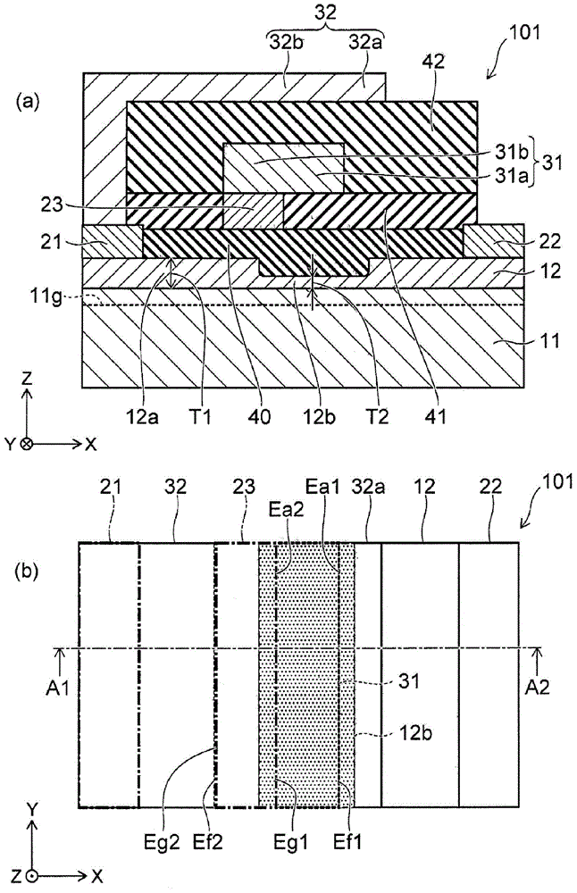
[0020] figure 1 (a) and figure 1 (b) is a schematic diagram illustrating the semiconductor device of the first embodiment.
[0021] figure 1 (a) is a schematic cross-sectional view of the semiconductor device 101, figure 1 (b) is a plan view of the semiconductor device 101.
[0022] figure 1 (a) Yes figure 1 (b) A cross-sectional view of line A1-A2 shown. figure 1 (b) is from figure 1 (a) The top view viewed from above.
[0023] The semiconductor device 101 is a HEMT (High Electron Mobility Transistor) made of, for example, a nitride semiconductor.
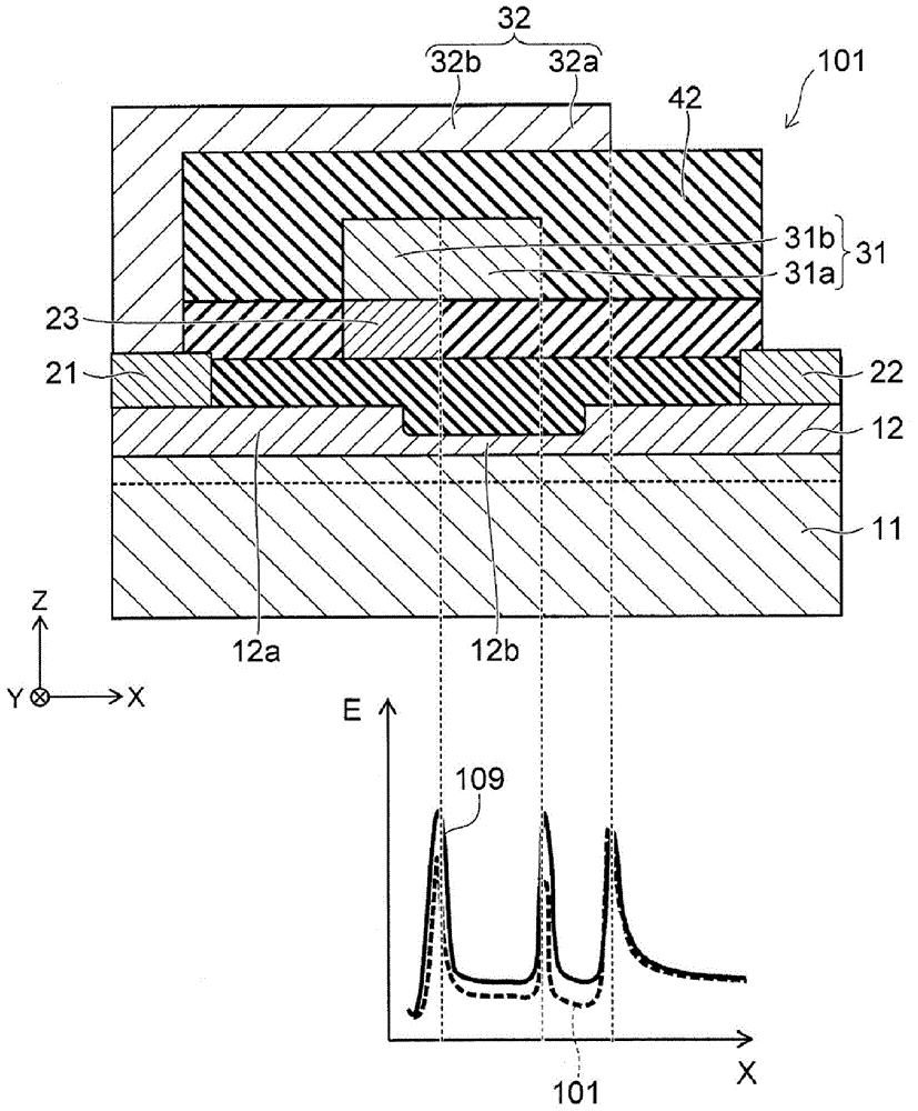
[0024] Such as figure 1 As shown in (a), the semiconductor device 101 includes a first semiconductor layer 11, a second semiconductor layer 12, a source electrode 21, a drain electrode 22, a gate electrode 23, a gate insulating film 40, and interlayer insulating films 41 and 42 , The first field plate electrode (FP electrode 31), and the second field plate electrode (FP electrode 32).
[0025] In addition, in figure 1 In the plan view of (...
no. 2 approach
[0080] Image 6 It is a schematic cross-sectional view illustrating the semiconductor device of the second embodiment.
[0081] Image 6 In the illustrated semiconductor device 105, the second semiconductor layer 12 has a multilayer structure. Regarding other configurations, the same components as those described for the semiconductor device 101 are assigned the same reference numerals, and descriptions thereof will be omitted.
[0082] The second semiconductor layer 12 has a laminated structure, and includes the first to third layers 13a to 13c.
[0083] The first layer 13a is disposed on the first semiconductor layer 11 and is in contact with the first semiconductor layer 11. The first layer 13a contains Al x2 Ga 1-x2 N(x1
[0084] The second layer 13b is disposed on the first layer 13a and is in contact with the first layer 13a. The second layer 13b is an AlN layer. The thickness of the second layer is 1 nm or more and 3 nm or less.
[0085] The third layer 13c is disposed...
PUM
| Property | Measurement | Unit |
|---|---|---|
| Thickness | aaaaa | aaaaa |
| Thickness | aaaaa | aaaaa |
| Thickness | aaaaa | aaaaa |
Abstract
Description
Claims
Application Information
 - R&D Engineer
- R&D Manager
- IP Professional
- Industry Leading Data Capabilities
- Powerful AI technology
- Patent DNA Extraction
Browse by: Latest US Patents, China's latest patents, Technical Efficacy Thesaurus, Application Domain, Technology Topic, Popular Technical Reports.
© 2024 PatSnap. All rights reserved.Legal|Privacy policy|Modern Slavery Act Transparency Statement|Sitemap|About US| Contact US: help@patsnap.com


