Manufacturing method of printed circuit board

A technology of printed circuit board and manufacturing method, which is applied in the direction of printed circuit manufacturing, printed circuit, electrical components, etc., which can solve the problems of easy deviation, board surface scratches, easy bending, etc., and achieve the elimination of connection traces and accurate positioning Effect

Active Publication Date: 2016-10-19
AOSHIKANG TECH CO LTD
View PDF9 Cites 8 Cited by
  • Summary
  • Abstract
  • Description
  • Claims
  • Application Information

AI Technical Summary

Problems solved by technology

[0002] Light screen PCB circuit boards need to mount a large number of LED lights, and need to be closely arranged, so only four 1.0mm copper-free holes can be set, and it is impossible to make more space in the board to arrange suitable positioning holes
However, the 1.0mm pin is easy to bend, and the board surface will be scratched during the board loading process, and the production process is also prone to misalignment, resulting in a high defect rate

Method used


Image

  • Manufacturing method of printed circuit board
  • Manufacturing method of printed circuit board
  • Manufacturing method of printed circuit board

Examples


Embodiment Construction

[0020] A method for manufacturing a printed circuit board of the present invention will be further described in detail below in conjunction with specific embodiments and accompanying drawings.

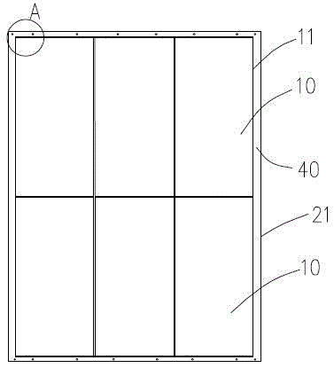
[0021] The printed circuit board (Printed Circuit Board, PCB) gong board method of the present invention is mainly applied to the inner part of the forming area (that is, the inner side of the process side) where no normal size (that is, a diameter greater than 2 mm) positioning hole is designed or only a diameter smaller than Or a PCB board with non-sinking copper holes equal to 1.5mm. When the diameter of the non-sinking copper hole is less than or equal to 1.5mm, it is not suitable as a positioning hole, the pin is easy to bend, the positioning is not accurate and the board surface is easy to scratch.

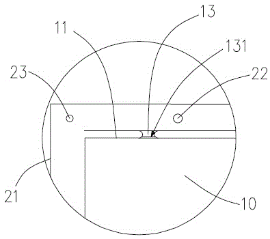
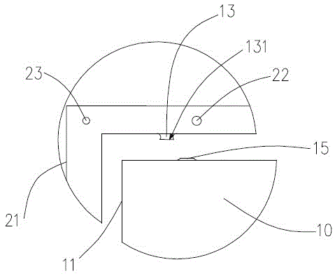
[0022] Please refer to figure 1 and figure 2 , in a preferred embodiment, figure 1 It is a schematic diagram of the structure of the PCB board in front of the gong board, figur...


PUM


Abstract

The invention relates to a manufacturing method of a printed circuit board. The manufacturing method is applicable to the printed circuit board with no positioning hole designed in the inner side of a technological side or only with non-electroplate-copper hole with the diameter smaller than or equal to 1.5 mm. The manufacturing method comprises the steps that V-cut production is carried out, the technological edge, close to the peripheral edge, of each unit of the printed circuit board is provided with at least two connection places with the length of 1-2 mm, the V-cut line of each connection place exceeds the technological edge by 0.1-0.2 mm, the remaining thickness of each connection place is 0.15-0.25 mm, and peripheral positioning holes are drilled near the connection places. According to the method, V-cut production is carried out on the PCB at first, the technological edge, close to the peripheral edge, of the PCB is provided with the connection places, the peripheral positioning holes are formed in the outer sides of the connection places and used for carrying out cutting operation, and it can be ensured that positioning is accurate and displacement is avoided.

Description

technical field [0001] The invention relates to a method for manufacturing a printed circuit board, in particular to a method for manufacturing a printed circuit board without a positioning hole larger than 1.5 mm in a forming board. Background technique [0002] Light-screen PCBs need to mount a large number of LED lights, and they need to be arranged closely. Therefore, only four 1.0mm copper-free holes can be set, and it is impossible to make more space in the board to arrange suitable positioning holes. However, the 1.0mm pins are easy to bend, and the board surface will be scratched during the board loading process, and the production process is also prone to misalignment, resulting in a high defect rate. If the user cannot adopt the V-cut method of increasing the process edge for production and does not accept abnormalities such as burrs on the edge of the board, it will not be able to use the punching method for production; in order to meet the needs of the customer's...

Claims


Application Information

Patent Timeline
Patent Type & Authority Applications(China)
IPC IPC(8): H05K3/00
CPCH05K3/0044
Inventor 黄海宏何高强黄勇周睿
Owner AOSHIKANG TECH CO LTD
Why Eureka
Try Eureka