Circuit substrate, display panel and display device

A technology for circuit substrates and display panels, applied in the field of electronics, can solve problems such as product quality hazards and product instability

Inactive Publication Date: 2016-11-09
BOE TECH GRP CO LTD +1
View PDF6 Cites 7 Cited by
  • Summary
  • Abstract
  • Description
  • Claims
  • Application Information

AI Technical Summary

Problems solved by technology

Potential damage is usually not found in the inspection of the production process...

Method used


Image

  • Circuit substrate, display panel and display device
  • Circuit substrate, display panel and display device
  • Circuit substrate, display panel and display device

Examples


Embodiment Construction

[0025] In order to make the purpose, technical solutions and advantages of the embodiments of the present invention more clear, the following will clearly and completely describe the technical solutions of the embodiments of the present invention in conjunction with the drawings of the embodiments of the present invention. Apparently, the described embodiments are only some of the embodiments of the present invention, but not all of them. Based on the described embodiments of the present invention, all other embodiments obtained by persons of ordinary skill in the art without creative efforts shall fall within the protection scope of the present invention.

[0026] Herein, the term "connected" includes direct connection or indirect connection between elements. Furthermore, it should be noted that although embodiments of the present invention are described herein in the context of array substrates, those skilled in the art will understand that the principles of the present inve...


PUM


Abstract

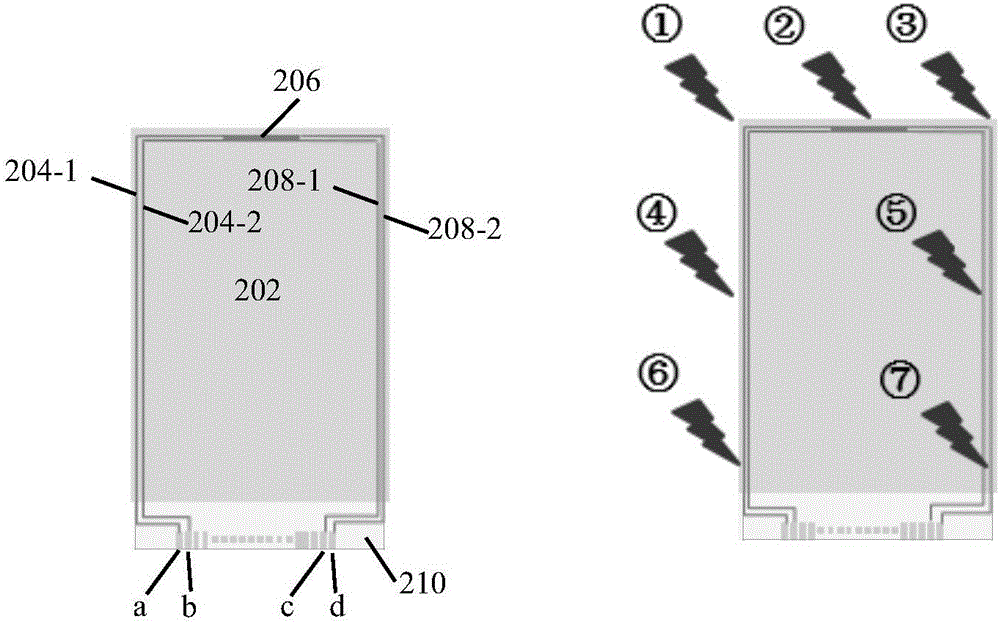
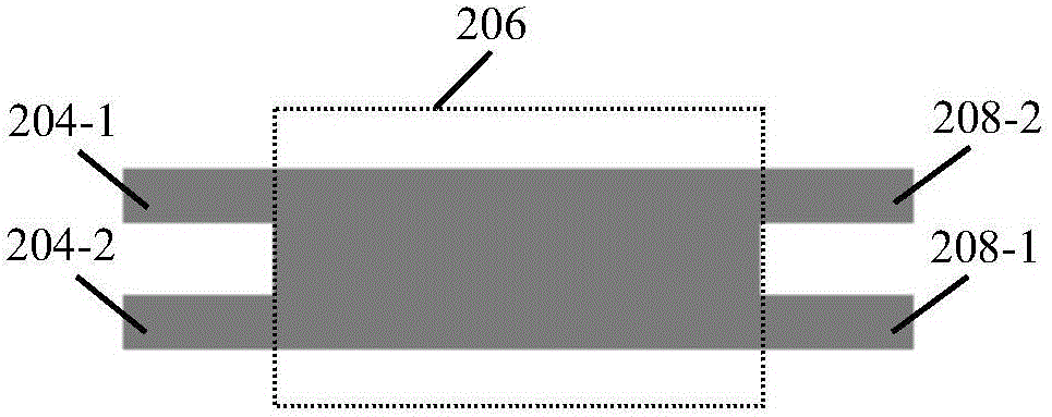
The embodiment of the invention relates to a circuit substrate, a display panel and a display device. The circuit substrate comprises a grounding protection circuit, wherein the grounding protection circuit comprises one or two parallelly-arranged first wires, a bridging portion and two parallelly-arranged second wires. The first wires, the bridging portion and the second wires are sequentially arranged along the periphery of the circuit substrate. One end of each first wire is grounded, and the other end of each first wire is electrically connected with the bridging portion. One end of each second wire is electrically connected with the bridging portion, and the other end of each second wire is grounded. The display panel comprises the circuit substrate. The display device comprises the display panel.

Description

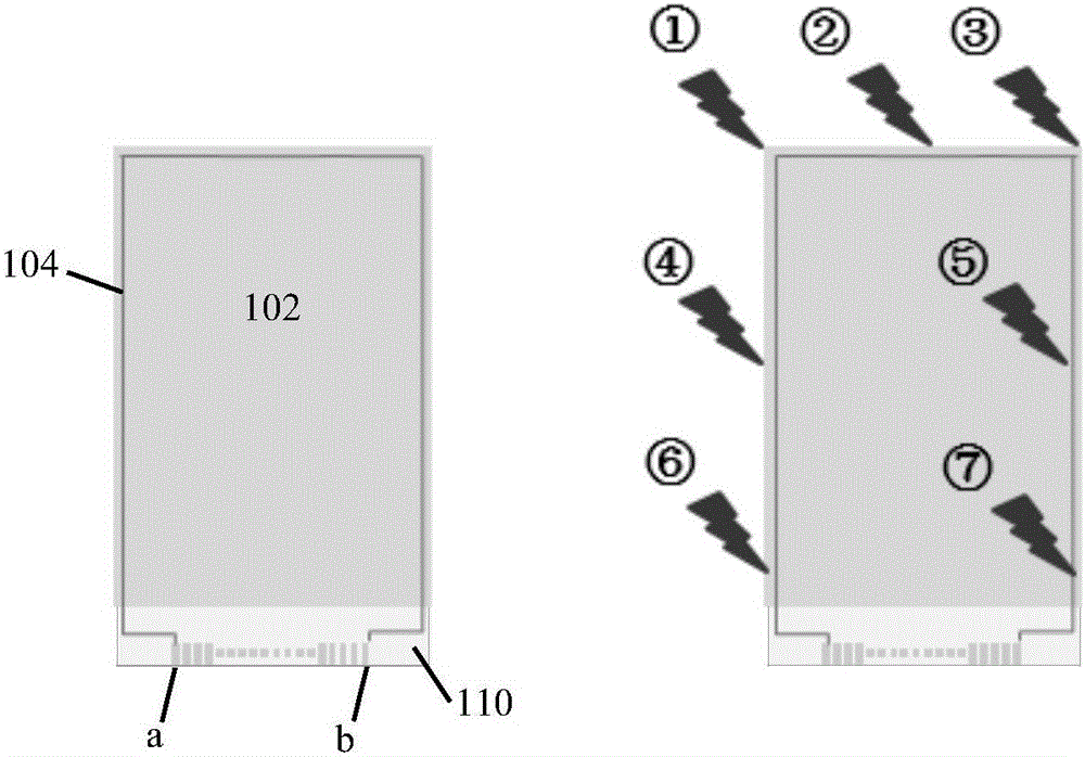
technical field [0001] Embodiments of the present invention relate to the field of electronics, and in particular to a circuit substrate, a display panel and a display device. Background technique [0002] There are two types of damage and damage caused by electrostatic discharge (ESD) to electronic products: sudden damage and potential damage. Sudden damage means that the device is severely damaged and its function is lost. This kind of damage can usually be found in the quality inspection of the production process. Latent damage means that the device is partially damaged, but the function has not been lost. Potential damage is usually not found in the inspection of the production process, which will make the product unstable and thus pose a greater hazard to product quality. Therefore, there is a demand for continuously improving the electrostatic protection performance of electronic products. Contents of the invention [0003] Embodiments of the present invention pr...

Claims


Application Information

Patent Timeline
IPC IPC(8): G02F1/1362
CPCG02F1/136204H01R13/6594H05K1/0259G02F1/1362G06F3/045H01R12/61H01R12/613H05K1/0215
Inventor 徐敬义张琨鹏任艳伟赵艳艳樊祎刘宇
Owner BOE TECH GRP CO LTD
Why Eureka
Try Eureka