Display panel and array substrate thereof

An array substrate and display panel technology, applied in nonlinear optics, instruments, optics, etc., can solve problems such as poor diffusion of pressed liquid crystals, and achieve the effect of reducing the risk of failure and avoiding the effect of falling over

Inactive Publication Date: 2016-11-09
TCL CHINA STAR OPTOELECTRONICS TECH CO LTD
View PDF6 Cites 0 Cited by
  • Summary
  • Abstract
  • Description
  • Claims
  • Application Information

AI Technical Summary

Problems solved by technology

[0004] The present invention provides a display panel and its array substrate to solve the technical problem in the prior art that there is a risk of poor diffusion of pressed liquid crystals

Method used


Image

  • Display panel and array substrate thereof
  • Display panel and array substrate thereof
  • Display panel and array substrate thereof

Examples


Embodiment Construction

[0033] The following will clearly and completely describe the technical solutions in the embodiments of the present invention in conjunction with the accompanying drawings in the embodiments of the present invention. Obviously, the described embodiments are only some of the embodiments of the present invention, not all of them. Based on the embodiments of the present invention, all other embodiments obtained by persons of ordinary skill in the art without making creative efforts belong to the protection scope of the present invention.

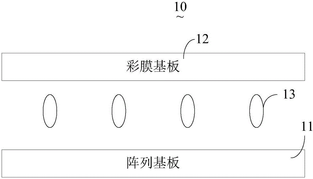
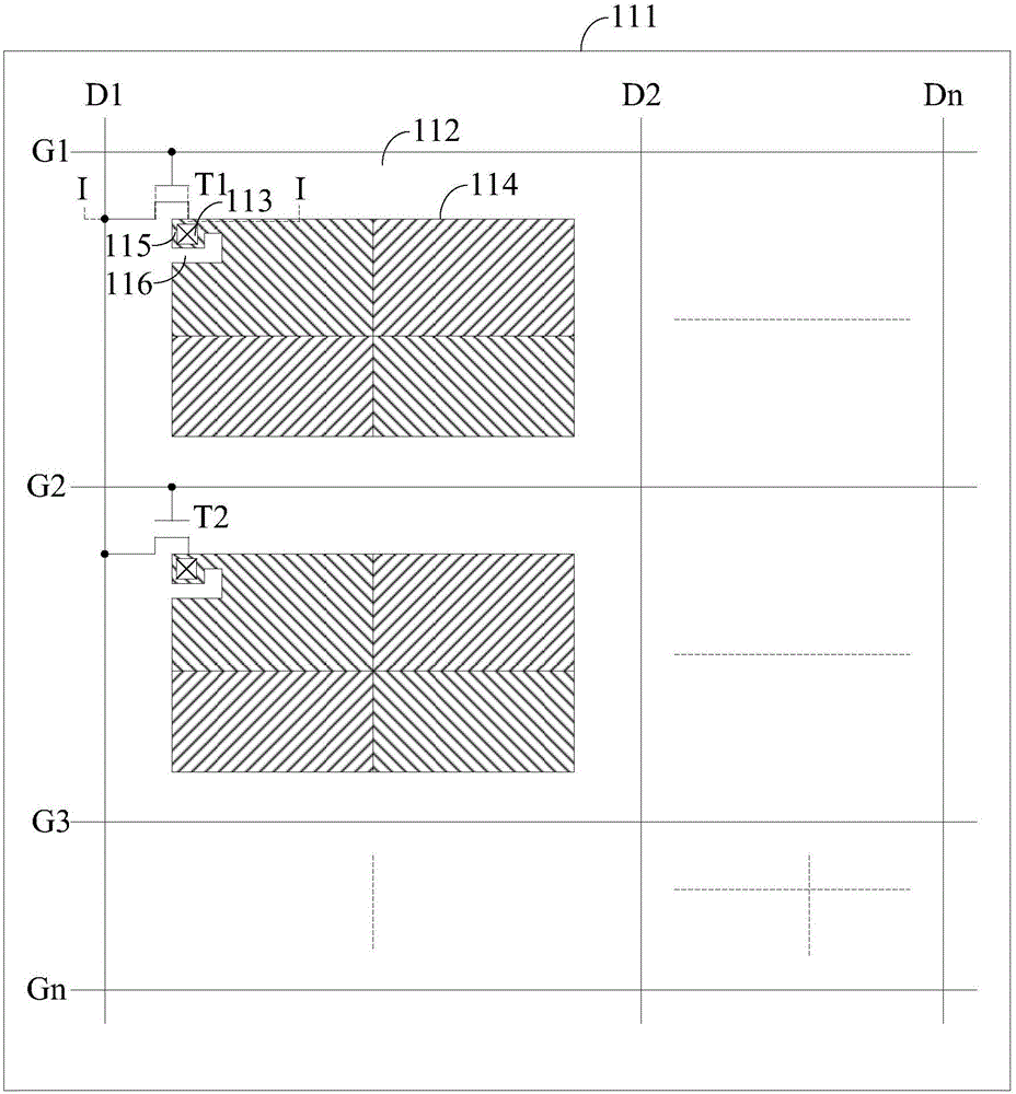
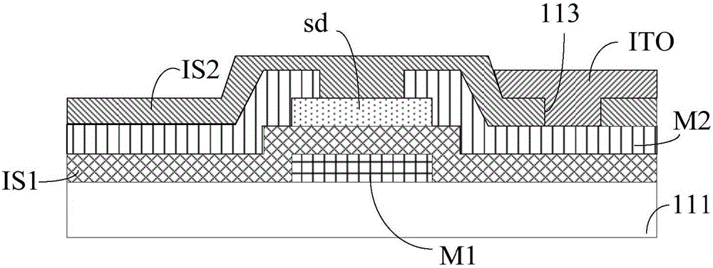
[0034] See Figure 1-3 as shown, figure 1 is a schematic structural view of the display panel of the first embodiment of the present invention; figure 2 yes figure 1 Schematic diagram of the structure of the array substrate; image 3 yes figure 2 Sectional view along I-I. Such as figure 1 As shown, the display panel 10 disclosed in this embodiment includes an array substrate 11, a color filter substrate 12, and a liquid crystal layer 13...


PUM


Abstract

The invention discloses a display panel and an array substrate thereof. The array substrate comprises multiple strips of scanning lines arranged on the substrate, and multiple strips of data lines arranged on the substrate and arranged alternately with the multiple scanning lines to form multiple pixel units. Each pixel unit comprises a pixel electrode. A via hole corresponds to a connection part of each pixel electrode. Each pixel electrode is provided with a hollow part. The hollow part is arranged adjacent to each connection part. By the above mode, the display panel and the array substrate thereof have following beneficial effects: liquid crystal molecules at other positions are prevented from being toppled such that risk of liquid crystal diffusion by pressing is reduced.

Description

technical field [0001] The present invention relates to the field of display technology, in particular to a display panel and an array substrate thereof. Background technique [0002] At present, in the pixel unit design of a conventional small-size, high-resolution liquid crystal display, in order to increase the transmittance of the pixel unit, it is usually adopted to arrange the via hole connecting the source electrode to the opening area in the corner of the opening. Since the electrodes connected by the via hole are the source metal layer and the pixel electrode layer, the terrain at the via hole is higher than other positions of the pixel electrode, resulting in a strong electric field. [0003] When the LCD screen is normally on, the liquid crystal at the via hole will be affected by the strong electric field and the high ground and fall to the via hole, causing the liquid crystal at other positions to fall in disorder, and there will be a risk of poor diffusion of t...

Claims


Application Information

Patent Timeline
Patent Type & Authority Applications(China)
IPC IPC(8): G02F1/1362G02F1/1343
CPCG02F1/136227G02F1/134309
Inventor 赵丽
Owner TCL CHINA STAR OPTOELECTRONICS TECH CO LTD
Why Eureka
Try Eureka